

Ayar Labs prepares for the era of co-packaged optics
The first of several articles on co-packaged optics.
Part 1: Ayar Labs
Ayar Labs is readying its co-packaged optics technology for scaled production in the second half of 2020. So says CEO Charlie Wuischpard who joined the start-up in late 2018 after it secured $24 million in funding to bring its products to market.
Co-packaged optics refers to the intimate coupling of optics with an ASIC in one package. Such tightly-coupled optics promises to overcome the growing system challenges associated with linking an ASIC’s high-speed signals to pluggable optics residing on a platform’s faceplate.
 Charlie Wuischpard Wuischpard joined Ayar Labs from Intel where he led the supercomputing segment within the company’s data centre group. Wuischpard also led Intel’s disaggregated rack initiative.
“In both these, silicon photonics plays a huge role in enabling future architectures and future designs,” he says.
Ayar Labs raised its funding after demonstrating successfully its optical designs: a silicon-photonics optical chiplet, dubbed Teraphy, and its Supernova external laser source.
“We are able to leverage the working chips to form new partnerships,” says Alexandra Wright-Gladstein, Ayar Labs’ chief strategy officer. “These partnerships are key because we are integrating very closely to partner chips within systems.”
Co-packaged optics
Wuischpard believes the tight coupling of optics with silicon is going to be ‘a big deal’.
He cites one equipment maker that told him that its next-generation servers will be optically integrated. “They are talking about tightly-integrated packaged optics in the server itself,” says Wuischpard.
Wuischpard joined Ayar Labs because he was attracted by its technology and the new opportunities co-packaged optics enable. But he admits questions remain as to how fast co-packaged optics will evolve and what the first applications will be.
 Alexandra Wright-Gladstein
“We have not been public about it but we have one big project with one of the majors where we are developing a prototype for the U.S. government,” says Wuischpard.
The prototype will demonstrate Ayar Labs’ chips coupled with the partner’s technology. “It is a co-packaged, co-design effort and while this is underway, we have deliverables throughout the rest of the year,” he says.
Input-output challenges
Ayar Labs highlights two opportunities driving interest in co-packaged optics. One is switch ICs used for networking within the data centre. The latest generation switch chips have a capacity of 12.8 terabits. The next generation 25.6-terabit switch chips are expected in the next year and a further capacity doubling to 51.2 terabits is expected by 2021 or 2022.
To achieve such a quadrupling in capacity, the switch chips must double the number of serialiser-deserialiser (serdes) circuits used for input-output (I/O) and double their speed. The 12.8-terabit devices use 256 serdes each at 50 gigabit-per-second (Gbps) achieved using 4-level pulse-amplitude modulation (PAM-4). A 51.2-terabit switch will use 512 serialiser-deserialisers (serdes), each operating at 100-gigabit PAM-4. Doubling the interface speed will reduce the reach of the electrical signals while doubling the number of serdes presents its own challenges. Both developments present signal-integrity challenges.
The products that will be created will be made by the silicon players, whether fabless or otherwise, and we are going to be a feature of that
The same issues apply to high-performance computing nodes that use graphics processing units (GPUs). Such GPUs are packed closely and use high-speed signalling to connect to memory and other computing nodes. The increasing bandwidth requirements of such systems represent another I/O challenge for electrical interfaces.
Does this mean that the market opportunity for co-packaged optics requires companies to become partner suppliers to the likes of Broadcom and Nvidia that dominate the respective switch and GPU markets?
“Generally that is correct; there are going to be a few large players who will be driving adoption,” says Wuischpard. But he highlights additional co-packaging opportunities.
One opportunity is the U.S. government and the system integrators that serve their opportunities. A second is the hyperscale data centre operators. “Ultimately, they are driving demand back to the Nvidias of this world,” says Wuischpard. “A lot of them are building their own custom silicon for certain workloads and use cases, particularly in AI.”
Optical design
Ayar Labs has demonstrated two optical chips. The Teraphy chiplet demonstrator crams three 400-gigabit receivers and five 400-gigabit transmitters, each using 16, 25-gigabit channels.
An external laser is used as the light source to feed the Teraphy chiplets. The 6.4 terabit Supernova module uses a source that can enable up to 256 data channels. Using an external laser source means it is not co-packaged alongside a hot chip thereby avoiding laser reliability concerns.
The Teraphy prototype includes optical macros only and Wright-Gladstein points out that its future product chiplet will also include electrical interfaces to enable the chiplet to communicate with the SoC’s serdes. The product chiplet will also have a matching number of optical transmitters and receivers.
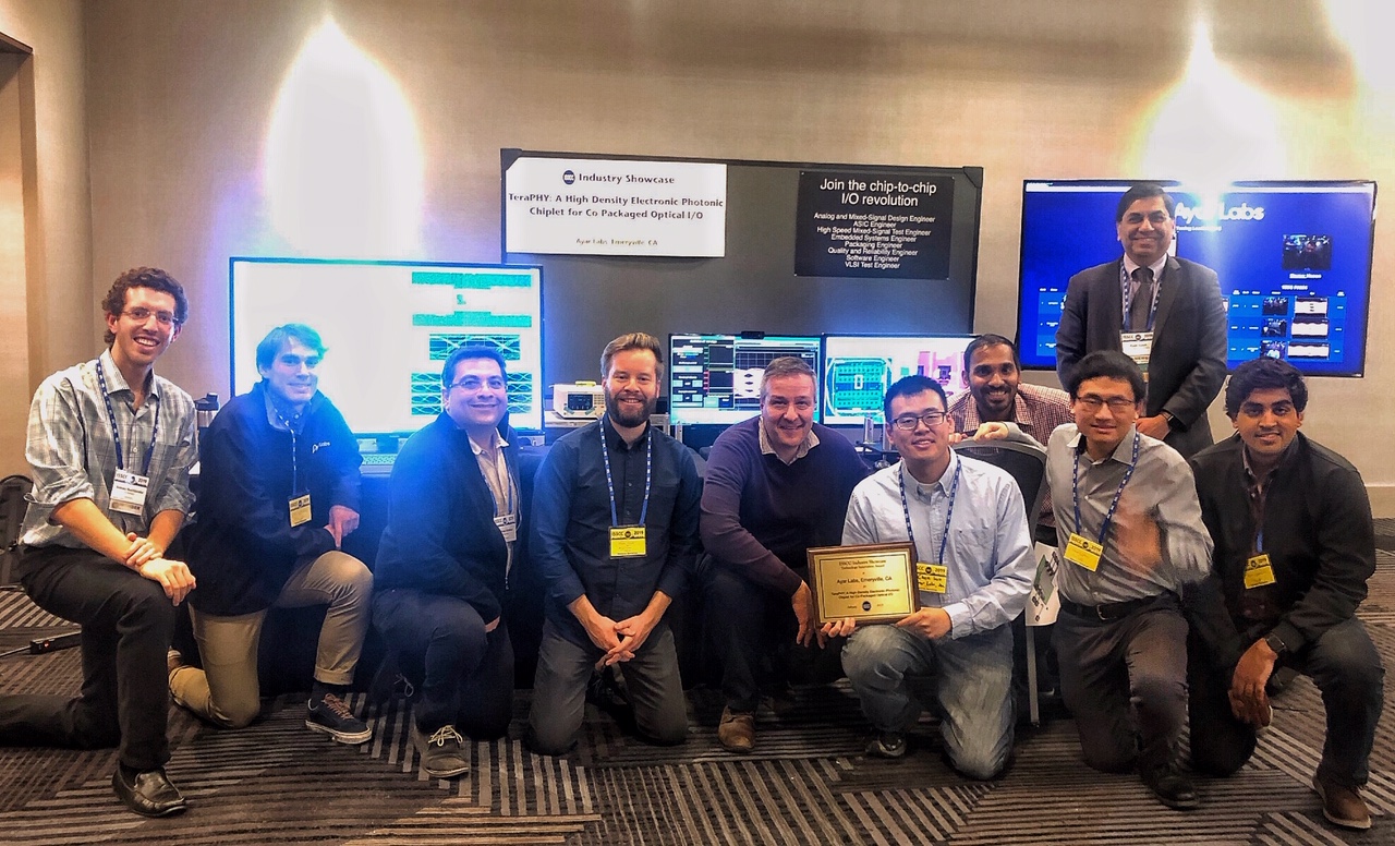 Ayar Labs won a technology innovation award at the recent IEEE ISSCC show after demonstrating the Teraphy sending a 100-gigabit 4-level pulse-amplitude modulation (PAM-4) signal.
Wright-Gladstein says that there are certain specifications an optical chiplet in a high-throughput design, such as a 51.2-terabit or even greater capacity switch package, needs to target. The targets include a bandwidth-density of greater than 100 gigabit-per-second per millimetre squared (Gbps/mm2) and a power efficiency below 2 picoJoules-per-bit (pJ/b). This means the aggregate I/O chiplets should consume no more than 100W. The optics, because it is co-packaged with the chip, should also be able to operate at high temperatures up to 125oC.
Ayar Labs says its prototype design desmonstrates the ability to more than meet these specifications. The design offers an in-package transmitter bandwidth density of 1Tbps/ mm2, a transmitter energy consumption under 1pJ/b, while the chiplets will be qualified to operate at 125oC.
Given that co-packaged optics is still a nascent market, designs are inevitably custom. “The industry would benefit from having standards in the co-packaged arena, not just for optics but other chiplets,” says Wuischpard.
On the networking side, such as switch chips, the interfaces are serial but certain applications require parallel interfaces. Accordingly, the development of standards for both styles of interface would be beneficial, he says.
Wuischpard identifies three areas likely to drive early adoption of co-packaged optics: specialised government computers that have huge bandwidth requirements, high-performance computing applications including AI, and networking applications.
But co-packaged optics will be challenging technically and will change the existing supply chain. Wuischpard highlights three distinct layers: the silicon and packaging players, the system builders, and the end users. Ayar Labs is in discussion with all three.
“The products that will be created will be made by the silicon players, whether fabless or otherwise, and we are going to be a feature of that,” says Wuischpard. “Our selling is likely going to be to a silicon provider or a packager and they are going to be working with the ecosystem.”
He also does not rule out selling directly to an end user such as a hyperscaler that has the resources to create their own designs.
The discussion regarding the target specifications was edited after publication.
 Post a Comment
Reader Comments