

Switch chips not optics set the pace in the data centre
Broadcom is doubling the capacity of its switch silicon every 18-24 months, a considerable achievement given that Moore’s law has slowed down.
Last December, Broadcom announced it was sampling its Tomahawk 3 - the industry’s first 12.8-terabit switch chip - just 14 months after it announced its 6.4-terabit Tomahawk 2.
 Rochan SankarSuch product cycle times are proving beyond the optical module makers; if producing next-generation switch silicon is taking up to two years, optics is taking three, says Broadcom.
“Right now, the problem with optics is that they are the laggards,” says Rochan Sankar, senior director of product marketing at switch IC maker, Broadcom. “The switching side is waiting for the optics to be deployable.”
The consequence, says Broadcom, is that in the three years spanning a particular optical module generation, customers have deployed two generations of switches. For example, the 3.2-terabit Tomahawk based switches and the higher-capacity Tomahawk 2 ones both use QSFP28 and SFP28 modules.
In future, a closer alignment in the development cycles of the chip and the optics will be required, argues Broadcom.
Switch chips
Broadcom has three switch chip families, each addressing a particular market. As well as the Tomahawk, Broadcom has the Trident and Jericho families (see table).
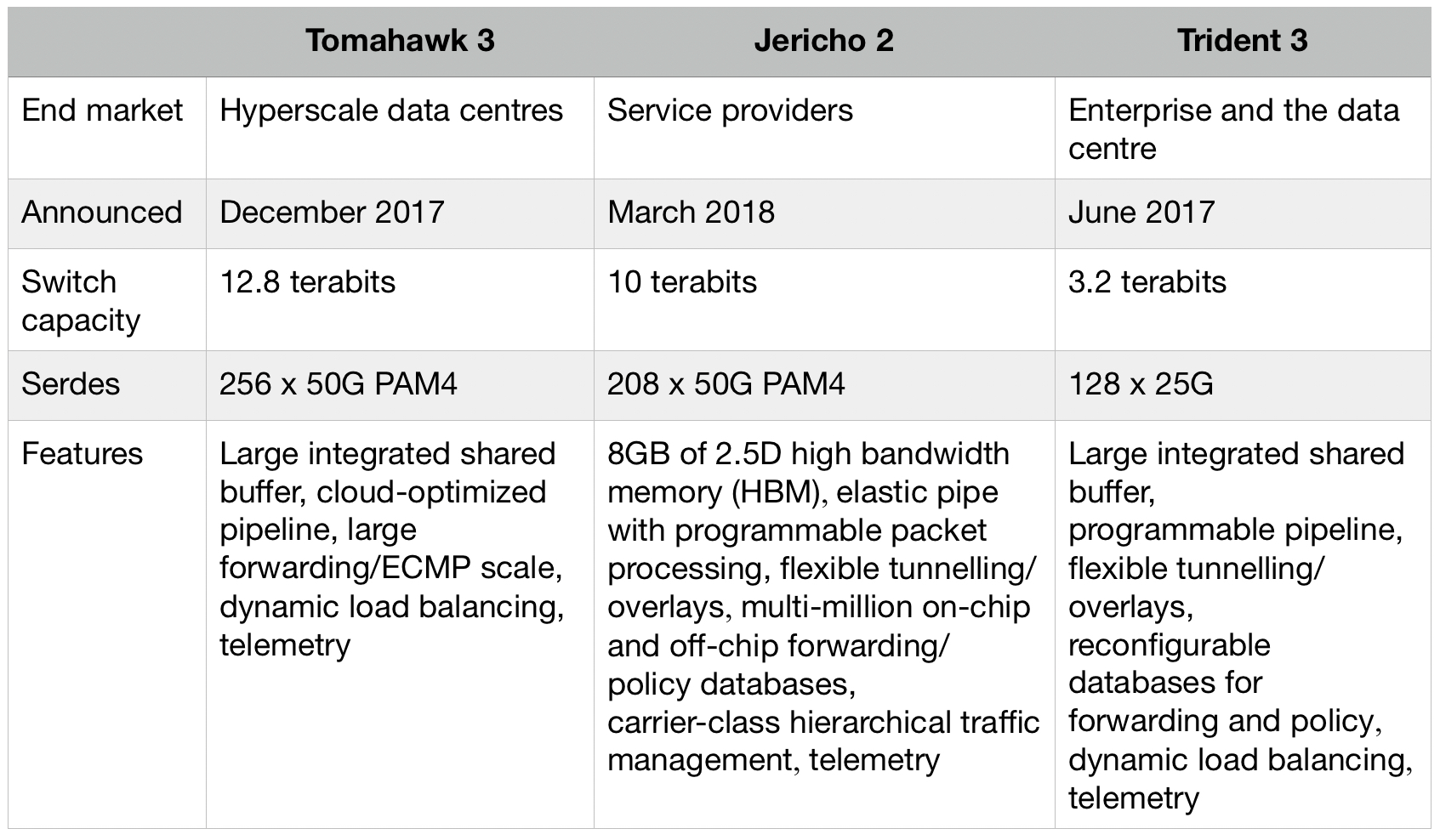
All three chips are implemented using a 16nm CMOS process. Source: Broadcom/ Gazettabyte.
“You have enough variance in the requirements such that one architecture spanning them all is non-ideal,” says Sankar.
The Tomahawk is a streamlined architecture for use in large-scale data centres. The device is designed to maximise the switching capacity both in terms of bandwidth-per-dollar and bandwidth-per-Watt.
“The hyperscalers are looking for a minimalist feature set,” says Sankar. They consider the switching network as an underlay, a Layer 3 IP fabric, and they want the functionality required for a highly reliable interconnect for the compute and storage, and nothing more, he says.
Right now, the problem with optics is that they are the laggards
Production of the Tomahawk 3 integrated circuit (IC) is ramping and the device has already been delivered to several webscale players and switch makers, says Broadcom.
The second, Trident family addresses the enterprise and data centres. The chip includes features deliberately stripped from the Tomahawk 3 such as support for Layer 2 tunnelling and advanced policy to enforce enterprise network security. The Trident also has a programmable packet-processing pipeline deemed unnecessary inlarge-scale data centres.
But such features are at the expense of switching capacity. “The Trident tends to be one generation behind the Tomahawk in terms of capacity,” says Sankar. The latest Trident 3 is a 3.2-terabit device.
The third, Jericho family is for the carrier market. The chip includes a packet processor and traffic manager and comes with the accompanying switch fabric IC dubbed Ramon. The two devices can be scaled to create huge capacity IP router systems exceeding 200 terabits of capacity. “The chipset is used in many different parts of the service provider’s backbone and access networks,” says Sankar. The Jericho 2, announced earlier this year, has 10 terabits of capacity.
Trends
Broadcom highlights several trends driving the growing networking needs within the data centre.
One is how microprocessors used within servers continue to incorporate more CPU cores while flash storage is becoming disaggregated. “Now the storage is sitting some distance from the compute resource that needs very low access times,” says Sankar.
The growing popularity of public cloud is also forcing data centre operators to seek greater servers utilisation to ‘pack more tenants per rack’.
There are also applications such as deep learning that use other computing ICs such as graphics processor units (GPUs) and FPGAs. “These push very high bandwidths through the network and the application creates topologies where any element can talk to any element,” says Sankar. This requires a ‘flat’ networking architecture that uses the fewest networking hops to connect the communicating nodes.
Such developments are reflected in the growth in server links to the first level or top-of-rack (TOR) switches, links that have gone from 10 to 25 to 50 and 100 gigabits. “Now you have the first 200-gigabit network interface cards coming out this year,” says Sankar.
Broadcom has been able to deliver 12.8 terabits-per-second in 16nm, whereas some competitors are waiting for 7nm
Broadcom says the TOR switch is not the part of the data centre network experiencing greatest growth. Rather, it is the layers above - the leaf-and-spine switching layers - where bandwidth requirements are accelerating the most. This is because the radix - the switch’s inputs and outputs - is increasing with the use of equal-cost multi-path (ECMP) routing. ECMP is a forwarding technique to distribute the traffic over multiple paths of equal cost to a destination port. “The width of the ECMP can be 4-way, 8-way and 16-way,” says Sankar. “That determines the connectivity to the next layer up.”
It is such multi-layered leaf-spine architectures that the Tomahawk 3 switch silicon addresses.
Tomahawk 3
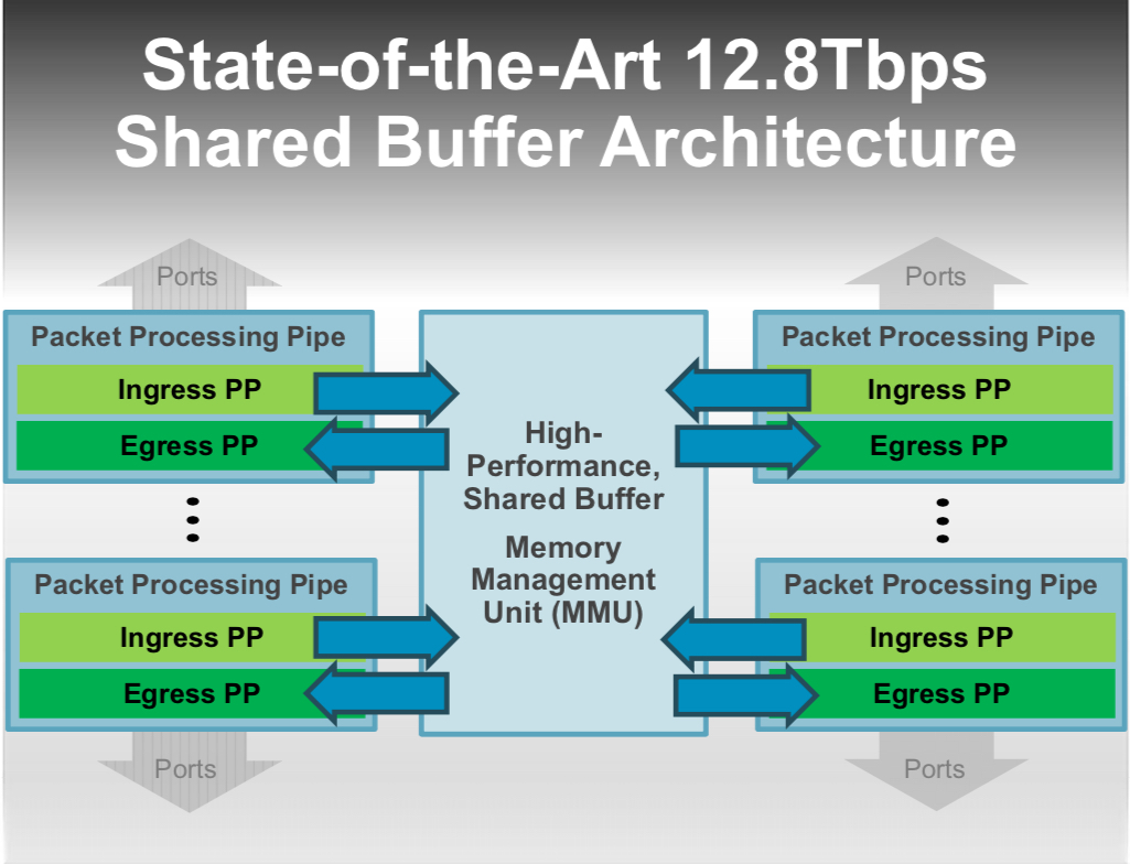
The Tomahawk 3 is implemented using a 16nm CMOS process and features 256 50-gigabit PAM-4 serialiser-deserialiser (serdes) interfaces to enable the 12.8-terabit throughput.
“Broadcom has been able to deliver 12.8 terabits-per-second in 16nm, whereas some competitors are waiting for 7nm,” says Bob Wheeler, vice president and principal analyst for networking at the Linley Group.
Sankar says Broadcom undertook significant engineering work to move from the 16nm Tomahawk 2’s 25-gigabit non-return-to-zero serdes to a 16nm-based 50G PAM-4 design. The resulting faster serdes design requires only marginally more die area while reducing the gigabit-per-Watt measure by 40 percent.
The Tomahawk 3 also features a streamlined packet-processing pipeline and improved shared buffering. In the past, a switch chip could implement one packet-processing pipeline, says Wheeler. But at 12.8 terabit-per-second (Tbps), the aggregate packet rate exceeds the capacity of a single pipeline. “Broadcom implements multiple ingress and egress pipelines, each connected with multiple port blocks,” says Wheeler. The port blocks include MACs and serdes. “The hard part is connecting the pipelines to a shared buffer, and Broadcom doesn’t disclose details here.”
 Source: Broadcom.
The chip also has telemetry support that exposes packet information to allow the data centre operators to see how their networks are performing.
Adopting a new generation of switch silicon also has system benefits.
One is reducing the number of hops between endpoints to achieve a lower latency. Broadcom cites how a 128x100 Gigabit Ethernet (GbE) platform based on a single Tomahawk 3 can replace six 64x100GbE switches in a two-tier arangement. This reduces latency by 60 percent, from 1 microsecond to 400 nanoseconds.
There are also system cost and power consumption benefits. Broadcom uses the example of Facebook’s Backpack modular switch platform. The 8 rack unit (RU) chassis uses two tiers of switches - 12 Tomahawk chips in total. Using the Tomahawk 3, the chassis can be replaced with a 1RU platform, reducing the power consumption by 75 percent and system cost by 85 percent.
Many in the industry have discussed the possibility of using the next 25.6-terabit generation of switch chip in early trials of in-package optics
Aligning timelines
Both the switch-chip vendors and the optical module players are challenged to keep up with the growing networking capacity demands of the data centre. The fact that next-generation optics takes about a year longer than the silicon is not new. It happened with the transition from 40-gigabit QSFP+ to 100-gigabit QSFP28 optical modules and now from the 100-gigabit QSFP28 to 200 gigabit QSFP56 and 400-gigabit QSFP-DD production.
“400-gigabit optical products are currently sampling in the industry in both OSFP and QSFP-DD form factors, but neither has achieved volume production,” says Sankar.
Broadcom is using 400-gigabit modules with its Tomahawk 3 in the lab, and customers are doing the same. However, the hyperscalers are not deploying Tomahawk-3 based data center network designs using 400-gigabit optics. Rather, the switches are using existing QSFP28 interfaces, or in some cases 200-gigabits optics. But 400-gigabit optics will follow.
The consequence of the disparity in the silicon and optics development cycles is that while the data centre players want to exploit the full capacity of the switch once it becomes available, they can’t. This means the data centre upgrades conducted - what Sankar calls ‘mid-life kickers’ - are costlier to implement. In addition, given that most cloud data centres are fibre-constrained, doubling the number of fibres to accommodate the silicon upgrade is physically prohibitive, says Broadcom.
“The operator can't upgrade the network any faster than the optics cadence, leading to a much higher overall total cost of ownership,” says Sankar. They must scale out to compensate for the inability to scale up the optics and the silicon simultaneously.
Optical I/O
Scaling the switch chip - its input-output (I/O) - presents its own system challenges. “The switch-port density is becoming limited by the physical fanout a single chip can support, says Sankar: “You can't keep doubling pins.”
It will be increasingly challenging to increase the input-output (I/O) to 512 or 1024 serdes in future switchchips while satisfying the system link budget, and achieving both in a power-efficient manner. Another reason why aligning the scaling of the optics and the serdes speeds with the switching element is desirable, says Broadcom.
Broadcom says electrical interfaces will certainly scale for its next-generation 25.6-terabit switch chip.
Linley Group’s Wheeler expects the 25.6-terabit switch will be achieved using 256 100-gigabit PAM4 serdes. “That serdes rate will enable 800 Gigabit Ethernet optical modules,” he says. “The OIF is standardising serdes via CEI-112G while the IEEE 802.3 has the 100/200/400G Electrical Interfaces Task Force running in parallel.”
But system designers already acknowledge that new ways to combine the switch silicon and optics are needed.
“One level of optimisation is the serdes interconnect between the switch chip and the optical module itself,” says Sankar, referring to bringing of optics on-board to shorten the electrical paths the serdes must drive. The Consortium of On-Board Optics (COBO) has specified just such an interoperable on-board optics solution.
“The stage after that is to integrate the optics with the IC in a single package,” says Sankar.
Broadcom is not saying which generation of switch chip capacity will require in-package optics. But given the IC roadmap of doubling switch capacity at least every two years, there is an urgency here, says Sankar.
The fact that there are few signs of in-package developments should not be mistaken for inactivity, he says: “People are being very quiet about it.”
Brad Booth, chair of COBO and principal network architect for Microsoft’s Azure Infrastructure, says COBO does not have a view as to when in-package optics will be needed.
Discussions are underway within the IEEE, OIF and COBO on what might be needed for in-package optics and when, says Booth: “One thing that many people do agree upon is that COBO is solving some of the technical problems that will benefit in-package optics such as optical connectivity inside the box.”
The move to in-package optics represents a considerable challenge for the industry.
“The transition and movement to in-package optics will require the industry to answer a lot of new questions that faceplate pluggable just doesn’t handle,” says Booth. “COBO will answer some of these, but in-package optics is not just a technical challenge, it will challenge the business-operating model.”
Booth says demonstrations of in-package optics can already be done with existing technologies. And given the rapid timelines of switch chip development, many in the industry have discussed the possibility of using the next 25.6-terabit generation of switch chip in early trials of in-package optics, he says.
There continues to be strong interest in white-box systems and strong signalling to the market to build white-box platforms
White boxes
While the dominant market for the Tomahawk family is the data centre, a recent development has been the use the 3.2-terabit Tomahawk chip within open-source platforms such as the Telecom Infra Project’s (TIP) Voyager and Cassini packet optical platforms.
Ciena has also announced its own 8180 platform that supports 6.4 terabits of switching capacity, yet Ciena says the 8180 uses a Tomahawk 3, implying the platform will scale to 12.8Tbps.
Niall Robinson,vice president, global business development at ADVA, a member of TIP and the Voyager initiative, makes the point that since the bulk of the traffic remains within the data centre, the packet optical switch capacity and the switch silicon it uses need not be the latest generation IC.
“Eventually, the packet-optical boxes will migrate to these larger switching chips but with some considerable time lag compared to their introduction inside the data centre,” says Robinson.
The advent of 400-gigabit client-port optics will drive the move to higher-capacity platforms such as the Voyager because it is these larger chips that can support 400-gigabit ports. “Perhaps a Jericho 2 at 9.6-terabit is sufficient compared to a Tomahawk 3 at 12.8-terabit,” says Robinson.
Edgecore Networks, the originator of the Cassini platform, says it too is interested in the Tomahawk 3 for its Cassini platform.
“We have a Tomahawk 3 platform that is sampling now,” says Bill Burger, vice president, business development and marketing, North America at Edgecore Networks, referring to a 12.8Tbps open networking switch that supports 32, 400-gigabit QSFP-DD modules that has been contributed to the Open Compute Project (OCP).
Broadcom’s Sankar highlights the work of the OCP and TIP in promoting disaggregated hardware and software. The initiatives have created a forum for open specifications, increased the number of hardware players and therefore competition while reducing platform-development timescales.
“There continues to be strong interest in white-box systems and strong signalling to the market to build white-box platforms,” says Sankar.
The issue, however, is the lack of volume deployments to justify the investment made in disaggregated designs.
“The places in the industry where white boxes have taken off continues to be the hyperscalers, and a handful of hyperscalers at that,” says Sankar. “The industry has yet to take up disaggregated networking hardware at the rate at which it is spreading at least the appearance of demand.”
Sankar is looking for the industry to narrow the choice of white-box solutions available and for the emergence of a consumption model for white boxes beyond just several hyperscalers.
 Post a Comment
Reader Comments