counter for iweb
Website
Silicon Photonics

Published book, click here

Wednesday
Jul052017

The era of cloud-scale routeing 

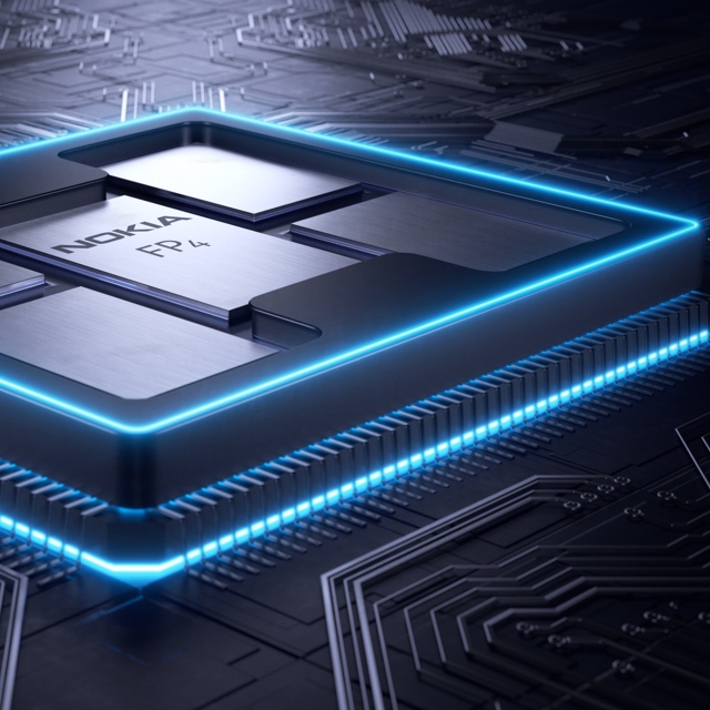
Nokia's FP4 p-chip. The multi-chip module shows five packages: the p-chip die surrounded by four memory stacks. Each stack has five memory die. The p-chip and memory stacks are interconnected using an interposer.
  • Nokia has unveiled the FP4, a 2.4 terabit-per-second network processor that has 6x the throughput of its existing FP3. 
  • The FP4 is a four-IC chipset implemented using 16nm CMOS FinFET technology. Two of the four devices in the chipset are multi-chip modules.
  • The FP4 uses 56 gigabit-per-second serial-deserialiser (serdes) technology from Broadcom, implemented using PAM-4 modulation. It also supports terabit flows.
  • Nokia announced IP edge and core router platforms that will use the FP4, the largest configuration being a 0.58 petabit switching capacity router. 

Much can happen in an internet minute. In that time, 4.1 million YouTube videos are viewed, compared to 2.8 million views a minute only last year. Meanwhile, new internet uses continue to emerge. Take voice-activated devices, for example. Amazon ships 50 of its Echo devices every minute, almost one a second.

Given all that happens each minute, predicting where the internet will be in a decade’s time is challenging. But that is the task Alcatel-Lucent’s (now Nokia’s) chip designers set themselves in 2011 after the launch of its FP3 network processor chipset that powers its IP-router platforms.

Six years on and its successor - the FP4 - has just been announced. The FP4 is the industry’s first multi-terabit network processor that will be the mainstay of Nokia’s IP router platforms for years to come.

Click to read more ...

Wednesday
Jul052017

Meeting the many needs of data centre interconnect

High capacity. Density. Power efficiency. Client-side optical interface choices. Coherent transmission. Direct detection. Open line system. Just some of the requirements vendors must offer to compete in the data centre interconnect market.

“A key lesson learned from all our interactions over the years is that there is no one-size-fits-all solution,” says Jörg-Peter Elbers, senior vice president of advanced technology, standards and IPR at ADVA Optical Networking. “What is important is that you have a portfolio to give customers what they need.”

 Jörg-Peter Elbers

Click to read more ...

Thursday
Jun222017

The OIF’s 400ZR coherent interface starts to take shape

Part 2: Coherent developments

The Optical Internetworking Forum’s (OIF) group tasked with developing two styles of 400-gigabit coherent interface is now concentrating its efforts on one of the two.

When first announced last November, the 400ZR project planned to define a dense wavelength-division multiplexing (DWDM) 400-gigabit interface and a single wavelength one. Now the work is concentrating on the DWDM interface, with the single-channel interface deemed secondary. 

Karl Gass"It [the single channel] appears to be a very small percentage of what the fielded units would be,” says Karl Gass of Qorvo and the OIF Physical and Link Layer working group vice chair, optical, the group responsible for the 400ZR work.

The likelihood is that the resulting optical module will serve both applications. “Realistically, probably both [interfaces] will use a tunable laser because the goal is to have the same hardware,” says Gass.   

Click to read more ...

Tuesday
Jun202017

Coherent optics players target the network edge for growth

Part 1: Coherent developments

The market for optical links for reaches between 10km and 120km is emerging as a fierce battleground between proponents of coherent and direct-detection technologies. 

Interest in higher data rates such as 400 gigabits is pushing coherent-based optical transmission from its traditional long-distance berth to shorter-reach applications. “That tends to be where the growth for coherent has come from as it has migrated from long-haul to metro,” says Tom Williams, senior director of marketing at Acacia Communications, a coherent technology supplier. 


Source: Acacia Communications, Gazettabyte

Williams points to the Optical Internetworking Forum’s (OIF) ongoing work to develop a 400-gigabit link for data centre interconnect. Dubbed 400ZR, the project is specifying an interoperable coherent interface that will support dense wavelength-division multiplexing (DWDM) links for distances of at least 80km.

Click to read more ...

Wednesday
Jun142017

Infinera unveils its next-gen packet-optical platforms 

  • Infinera has announced its first major metro product upgrade since it acquired Transmode in 2015.
  • The XTM II platforms use CFP2-DCO pluggable modules for the line-side optics, not Infinera’s photonic integrated circuit (PIC) technology.
  • Infinera’s XTM II achieves new levels of power efficiency by adopting CFP2-DCO pluggables and a distributed switch architecture.
  •  

    Source: Infinera

    Infinera has unveiled its latest metro products that support up to 200-gigabit wavelengths using CFP2-DCO pluggable modules.

    The XTM II platform family is designed to support growing metro traffic, low-latency services and the trend to move sophisticated equipment towards the network edge. Placing computing, storage and even switching near the network edge contrasts with the classical approach of backhauling traffic, sometimes deep within the network.

    Click to read more ...

    Monday
    Jun052017

    Creating a long-term view for the semiconductor industry

    The semiconductor industry is set for considerable change over the next 15 years.

    “We are at an inflection point in the history of the [chip] industry,” says Thomas Conte, an IEEE Fellow. “It will be very different and very diverse; there won’t be one semiconductor industry.” 


    Conte (pictured) is co-chair of the IEEE Rebooting Computing initiative that is sponsoring the International Roadmap of Devices and Systems (IRDS) programme. The IRDS is defining technology roadmaps over a 15-year horizon and in November will publish its first that spans nine focus areas. (See The emergence of the IRDS, below).

    Click to read more ...

    Wednesday
    May312017

    Packaging silicon photonics using passive alignment  

    • An Israeli start-up is tackling a key packaging challenge for silicon photonics

    Teramount has developed a way to simplify the packaging of silicon photonics chips. Instead of using active alignment whereby an external laser is required to carefully align a fibre to the optical die, the Israeli start-up has developed a technology that allows passive alignment.  


    Hesham Taha“If we want silicon photonics to ramp up to volume, it has to meet CMOS standards both in terms of fabrication and packaging,” says Hesham Taha, Teramount's CEO.

    Taha worked at a company developing atomic force microscopy systems before co-founding Teramount. "We got to know of the problem of injecting light into a waveguide and were surprised that the industry was still using active alignment," he says.

    Click to read more ...