

Ranovus outlines its co-packaged optics plans
Part 2: Odin technology
Ranovus has tested a chiplet that combines electronics and silicon photonics. Dubbed Odin 8, the monolithic design is targetting the co-packaged optics opportunity, enabling silicon chips to communicate optically.
The company is developing two such chiplets: the 800-gigabit Odin 8 and the higher-capacity Odin 32 that supports 3.2 terabits of traffic.
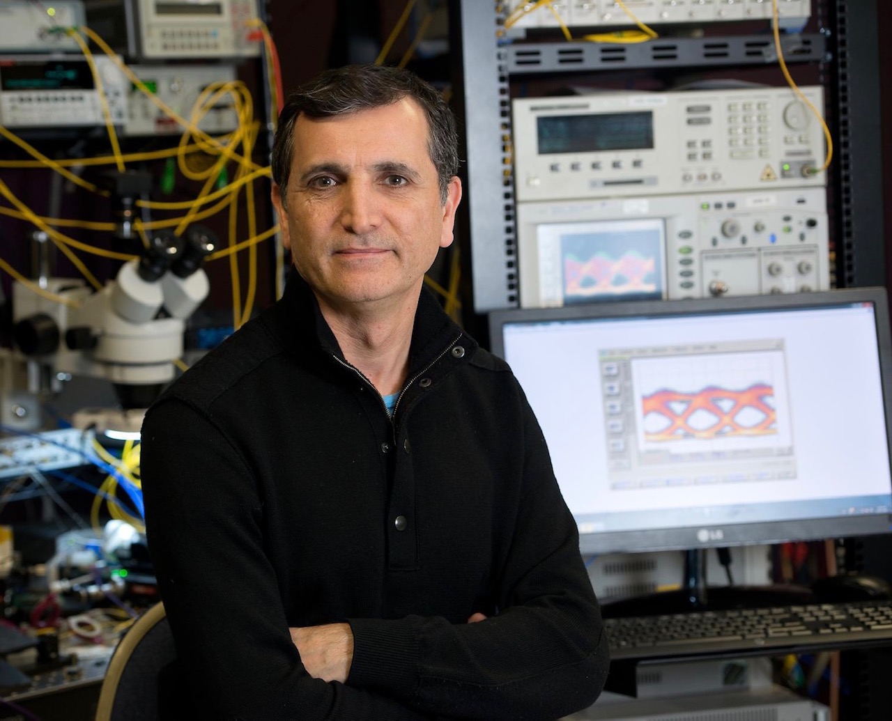 Hamid Arabzadeh
The first use of Odin 8 will be for 800-gigabit client-side modules. “We already have three lead customers for our 800-gigabit module business,” says Hamid Arabzadeh, CEO of Ranovus.
The 800-gigabit pluggable modules using the Odin 8 are expected to be generally available from late 2021.
Company
Founded in 2012, Ranovus is a late-stage start-up that has raised close to $100 million in funding. About half the sum is from venture capital firms and the rest is non-dilutive funding from sources including the Canadian government. An unnamed strategic investor also closed a deal with Ranovus late last year.
Ranovus has several core technologies including a multi-wavelength quantum-dot laser, a silicon photonics-based ring resonator, and driver and receiver electronics.
Ranovus is bullish about its ring-resonator - used for modulating and filtering light - and claims to own core intellectual property (IP). “We have spent a lot of time over the last eight years patenting quite a lot of the key fundamentals,” says Arabzadeh.
The first product Ranovus developed addresses the data centre interconnect market. The 200-gigabit direct-detection CFP2 pluggable module uses four wavelengths, each at 50 gigabits, and has a reach of 85km.
But looming competition from 400ZR, the OIF 400-gigabit coherent standard for data centre interconnect, caused Ranovus to shift strategy a couple of years ago and develop products for use within the data centre. To this aim, the company bolstered its team with senior management appointments.
Data centres
Ranovus’s Odin co-packaged optics solutions are aimed at servers and Ethernet switches deployed in data centres.
Machine learning and artificial intelligence are fueling traffic growth placing new demands on servers.
“GPUs, CPUs, memory and storage are configured using electrical interfaces, and the higher bandwidth requirements will eventually lead to optical interfaces,” says Arabzadeh. A graphics processing unit (GPU) is a class of processor suited to machine learning. Such chips are sold by companies such as Nvidia, AMD and Intel.
Server are also adopting a disaggregated design whereby the elements needed for computation - processing, memory and storage - are pooled separately. This addresses the changing nature of workloads and allows for the server components to be upgraded independently.
“If you look at workloads in the cloud, these differ,” says Arabzadeh. “Some require a lot of processing, others need a lot of memory accesses. So this entails moving to pooled compute, pooled memory and pooled storage; a monolithic server doesn’t meet all the needs.”
Arabzadeh cites as an example the Open Compute Project’s (OCP) Open Accelerator Module (OAM) that combines eight GPUs. GPUs work on tasks that are highly latency- and protocol-sensitive.
Each GPU has an electrical bus to connect to storage and memory and there are lots of communication between GPUs and between GPUs in different racks, says Arabzadeh. As speeds go up, any hop between GPUs has to be optical because electrical links won’t be able to support that.
“Our Odin platform - our biggest claim to fame - is its low latency of 0.4ns,” says Arabzadeh. “We have validated this with four major systems players and we have tested their devices with our product and shown that this latency doesn't impact any of the protocols they use.”
The second key market for co-packaged optics is data-centre networking. Here, Ethernet switch chip capacities are doubling every two years.
Last December, Broadcom started delivering its 25.6-terabit StrataXGS Tomahawk 4 switch-chip, while the Barefoot division of Intel has spoken of its 25.6-terabit coming soon and has hinted that its 51.2-terabit switch chip is close behind (see Part 1: Intel combines optics to its Tofino 2 switch chip)
A doubling in switch-chip capacity requires a doubling of input-output (I/O) where ever-faster signals need to go across a printed circuit board. This is both a design challenge and burns power. Bringing optics alongside the switch chip allows shorter-reach XSR serialiser-deserialisers (serdes) to be used, saving power.
Odin devices
The Odin 32 device comprises silicon photonics-based optics and driver, receiver and control electronics.
The electrical inputs to the Odin 32 are 100-gigabit 4-level pulse-amplitude modulation (PAM-4) signals while the optical output uses eight fibres, each carrying a 400-gigabit FR4. Each FR4 is made up of four, 100-gigabit wavelengths.
The laser used is external to the Odin 32 since the chiplet’s temperature and power dissipation is quite high. “Using an external laser is compliant with what Facebook and Microsoft have launched in their co-packaged optics document,” says Arabzadeh.
Ranovus has developed a socket-based design such that each Odin 32 device surrounding the ASIC can be easily clipped on and removed. Using 16 such Odin 32s delivers the I/O needed for a 51.2-terabit capacity switch chip (see photo below).
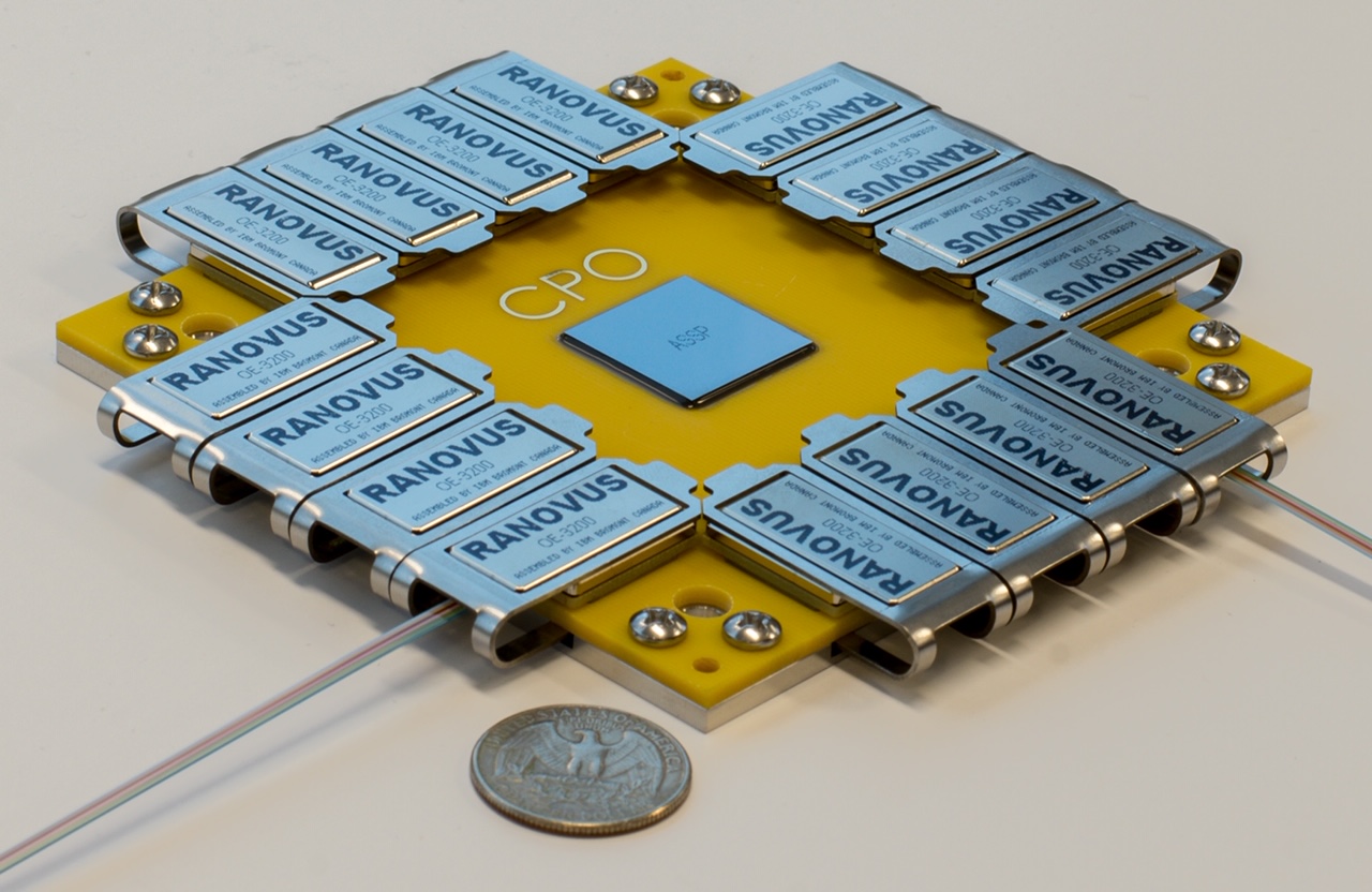 A co-packaged design: 16 chiplets providing optical I/O for the silicon chip. Source: Ranovus
The Odin 8 uses a similar design except the laser is integrated internally with the silicon-photonics and electronics.
For 800-gigabit pluggables, a PAM-4 chip is also used. Ranovus is working with two PAM-4 suppliers to co-package the PAM-4 chip with the Odin 8 device. “The optical engine, laser and the PAM-4 chip are all inside,” says Arabzadeh.
The company was going to demonstrate the Odin 8 implementing FR8 - sending eight 100-gigabit wavelengths on a single fibre - at the recent OFC show held in San Diego in March. But that was cancelled due to the COVID-19 pandemic.
Ranovus is targeting the 800-gigabit DR8 as its first market. “We see a market pull for the DR8 for 800 gigabits,” says Arabzadeh.
Addressing pluggables first with Odin 8 reduces the risk to end-customers keen to adopt the novel technology. “They can kick the tires on it, and then co-packaged optics will be a natural progression,” he says.
Pursuing both co-packaged optics and pluggable solutions also caters for the differing preferences of large-scale data centre players. Facebook and Microsoft are promoting co-packaged optics but at OFC both Google and Alibaba highlighted their preference for pluggable optics due to their flexibility and ease of use.
Cost and power
Ranovus says its co-packaged optics design halves the power consumption and reduces by three-quarters the cost of 100-gigabit pluggable modules.
Assuming a 100-gigabit module consumes 3-3.5W and costs $150 to $200, that implies the 3.2-terabit Odin 32 consumes between 48-56W and costs between $1,200 and $1,600.
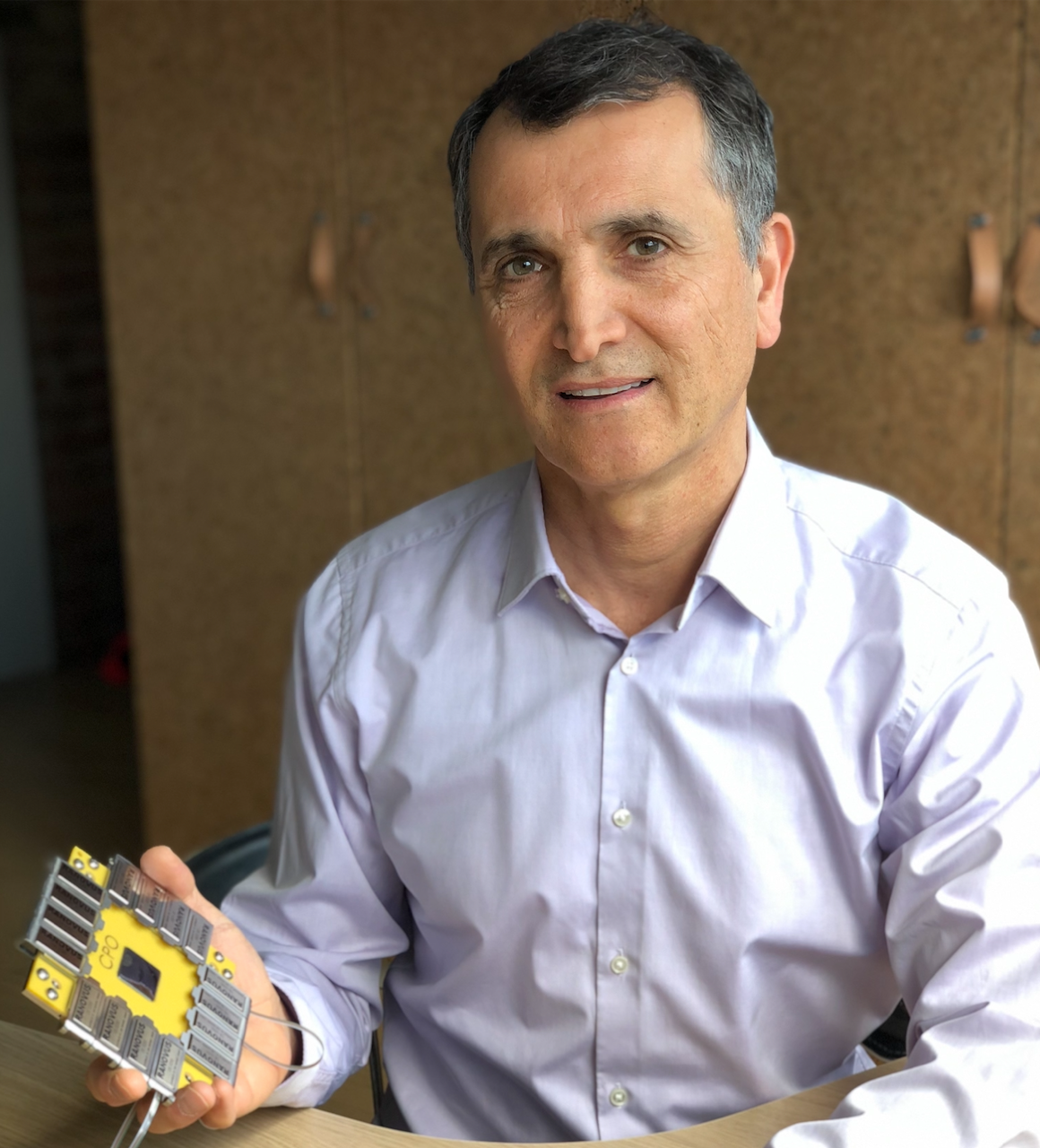 The CEO holding the multi-chip package, highlighting its size. Source: Ranovus.
One-hundred-gigabit modules rather than 400-gigabit modules were used for the comparison since 400-gigabit pluggables have yet to reach volume production. Accordingly, their pricing hasn’t stabilised nor has the power consumption had time to progressively come down.
“With the emergence of 100-gigabit serdes on switch ICs, we see the life of 400-gigabits, with 50-gigabit electronics going to 100-gigabit-per-wavelength, as being very short,” says Arabzideh. “We don't think they will reach critical mass in terms of power consumption and getting the cost down.”
Drivers for co-packaged optics
Ranovus, along with IBM, TE Connectivity and Senko Advanced Components, have formed a consortium to help firms embracing co-packaged optics to design and manufacture their products.
IBM brings its V-groove technology that is used for connecting fibre to the optics while TE Connectivity has worked with Ranovus on the packaging and the clip mechanism that fix in place the engines around the ASIC. Senko Advanced Components’s contribution is the design of the connector technology.
So what will trigger the adoption of co-packaged optics in the data centre? Arabzadeh cites three factors that will spur the technology’s introduction: power consumption reduction, miniaturisation and cost savings.
A key contributor to power reduction is the advent of 100-gigabit electrical interfaces so that, at last, the electrical signal rate matches 100-gigabit wavelengths.
The electrical input signalling rates have continued to lag behind pluggables’ 100-gigabit optical outputs. The advent of 100-gigabit electrical interfaces now means no rate-translation or ‘gearbox’ chip is needed, and that saves power.
“It becomes an electro-optic conversion without any multiplexing,” says Arabzadeh. “This is a key factor for co-packaged optics to be enabled.”
The second driver is systems miniaturisation. One parameter that is fixed is the upper size of switch chips. There is a certain die size above which yields start to go down. So the dimensions of the die will remain fixed with the move from 25.6-terabit to 51.2-terabit switch chips.
One issue that will help the design is the move from a 7nm to a 5nm CMOS process - allowing more transistors to be crammed in the fixed area. But each CMOS process shift is harder to achieve and is more costly.
But the issue remains getting the I/O signals off the chip to the front panel where the pluggable optics reside. For a 51.2-terabit switch chip, that is challenging.
The fixed size of the chip means the ever-higher-speed signals need to fan out from the chip to the very edges of the front panel. “This is going to be a nightmare; you are going to have retimers [chips] everywhere,” says Arabzadeh. By bringing the optics closer to the switch chip using co-packaged optics, the fan-out is lessened as the distances become shorter.
There is also the expectation that, given the size and number of the pluggable modules needed, a 51.2-terabit design will not fit into a one-rack-unit (1RU) platform. Using co-packaged optics, a 1RU 51.2-terabit switch is possible.
“There is a physics issue here: miniaturisation and not being able to fan out,” says Arabzadeh.
The third factor pushing towards co-packaged optics is cost reduction, argues Arabzadeh, pointing to Ranovus’s monolithic chiplet design: “The transistors are designed in the same mask as the silicon photonics”.
This means no wire-bonding is needed between the optics and separate electronics ICs, implemented using silicon germanium or CMOS.
“Each of these interfaces has to be optimised on an analogue level,” he says, adding that these factors increase the cost and power consumption. In contrast, a monolithic design means wafer-scale manufacturing can be used which benefits the economics.
“It is something we think will be cost-effective inside the data centre,” says Arabzadeh.
Availability
Engineering samples of the Odin 8 are expected in the first quarter of 2021, while general availability of 800-gigabit DR8 pluggables using the chiplet is due towards the end of next year.
But the timing is also dependent on the availability of PAM-4 chips. “There are not too many PAM-4 chips at 800 gigabits,” says Arabzadeh. The first PAM-4 designs so far announced use 7nm CMOS and despite that being state-of-the-art, Arabzadeh says lower-power chips are needed.
Meanwhile, the Odin 32 will tape-out in the third quarter of this year.
As for co-packaged optics, that is expected some six months to a year after 800-gigabit modules, says Ranovus: the second half of 2022.
 Post a Comment
Reader Comments