

Silicon photonics' second wave
- “I believe the field of silicon photonics is at a pivotal point of change and acceleration.”
- Professor Roel Baets, the winner of the 2020 John Tyndall Award, talks about what motivates his research and his interests.
Two concentric circles drawn in chalk are shown on-screen. So Professor Roel Baets open his plenary talk at the European Conference on Integrated Optics (ECIO) 2020, asking the online audience what is being shown.
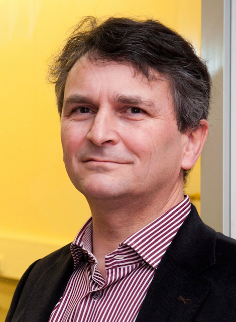 Professor Roel Baets
Suggestions come flooding in: the cross-section of an optical fibre, a silicon wafer, a ring resonator optical component and - the correct answer - a doughnut.
The image is from the front cover of Doughnut Economics: Seven Ways to Think Like a 21st-Century Economist by Kate Raworth, a UK professor of economics.
The author discusses how continual economic growth is out of kilter with the planet’s well-being and details alternative approaches. The “doughnut” represents a sweet-spot region ensuring sustainable growth.
Baets applied the book’s thinking to his plenary talk on the topic of silicon photonics research.
Research perspective
Baets’ research work focusses on the use of silicon photonics for applications other than telecom and datacom.
High-speed transceivers for telecom and datacom continue to drive silicon photonics, creating mature platforms and funding the technology’s development.
The two industries will also continue to drive silicon photonics for the coming decade but the picture is set to change. “There is huge potential for other markets; sensing, life sciences and medical being some of them,” he says.
Baets is director of the multidisciplinary Centre for Nano- and Biophotonics at Ghent University in Belgium. His research group comprises 90 staff, split between Ghent University and imec, the renowned R&D centre. “We are sort of a hybrid unit, part university and part imec,” he says.
His focus on the next wave of silicon photonics is partly due to a long-standing interest in biomedical engineering and because high-speed transceiver research is now mainstream.
“I have a big appetite to do something less evolutionary and more groundbreaking,” he says.
Applying the technology to do something helpful appeals to him: “Diagnosing diseases or for therapy of diseases, I feel that is more relevant.”
Background
Baets received the 2020 John Tyndall Award from The Optical Society (OSA) and the IEEE Photonics Society. The award is for his “seminal research in silicon photonics and for driving the foundry model in this field.”
Baets read electrical engineering at Ghent University where he also earned a masters degree. He gained a second masters at Stanford University in California.
“It sounds redundant but I had the privilege of doing a lot of things in terms of subjects that I hadn’t been able to do at Ghent so it was wonderful,” says Baets.
It was at Stanford that Baets pursued his interest in biomedical engineering. He also ‘fell in love’ with photonics after he met and worked with Joseph Goodman, whom he describes as the father of Fourier optics and statistical optics.
That set the course of his photonics research, while his interest in biomedical engineering remained. “And it [biomedical engineering] has popped up in recent years in combination with photonics,” he says.
Foundry model
Baets compares the progress of silicon photonics with that of the chip industry several decades ago.
In the 1970s, universities undertaking integrated circuit research had clean rooms but the growing sophistication of chip-making meant it became too costly.
“Universities and research groups had to give up having their own fabrication facilities for research,” he says.
The same happened within the chip industry, with few chip firms able to afford clean rooms resulting in the advent of foundries.
Even the semiconductor titan Intel, which built its fortune by leading the chip industry in CMOS process technology, is now considering foundries to make its chips.
A similar model is now playing out with integrated photonics.
“The microelectronics fab is an extremely expensive infrastructure,” says Baets. “Maintaining the process flow for certain platforms that enable you to combine [optical] functions on-chip takes quite a bit of diligence and therefore cost.”
This is why creating ‘open’ mechanisms whereby interested parties can gain access to such technology is so important.
“Even if you don’t have a fab in your backyard, there are places you can go to,” says Baets. “That was the essence behind starting ePIXfab.”
Baets helped found ePIXfab, the first global multi-project wafer service for silicon photonics, in 2006.
The idea of multi-project wafers is to aggregate photonic designs from many different users into one mask set before passing a wafer run through a fab. “Multi-project wafers is a cost-sharing process that is well established in electronics,” he says.
Platforms
The Kate Raworth book on sustainable growth was an eye-opener to many people, says Baets, given the topic was addressed by an economist rather than a climate-change scientist.
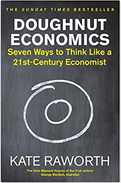
“Growth is important but there are other dimensions, and you need to find a sweet spot,” he says. “I couldn’t resist using this for my ECIO talk as a metaphor for the field of silicon photonics.”
Silicon photonics is at a turning point, he says, and it will be interesting to see how the field develops over the next five to ten years in terms of finding a way to create mature platforms serving different applications and markets.
The term platform refers to the entire chain of processes that happen in a microelectronics fab, starting with plain wafers and ending with diced chips.
When Baets talks about mature platforms he is referring to a standardised process flow where the basic components are well defined and where a user has some freedom in how the optical functions are connected. It should also be “open access”, similar to CMOS chip foundries.
The technology used for chip-making - the wafer-level processes and the infrastructure - is hugely expensive yet what it produces - the chips - are ‘insanely cheap’, says Baets
“Because of these special boundary conditions, you have to be careful in the research directions you choose,” he says. ”It doesn’t make sense to embark in a direction where it is hard to imagine how it would fit into a sustainable platform.“
This is the essence of his plenary talk.
For example, several places around the world have created a process flow that combines silicon nitride optical waveguides with standard silicon ones. This has only happened in the last couple of years.
“It is a beautiful example of how you can extend the richness of a platform to another level, thereby serving many new applications and customers,” he says.
Meanwhile, a current focus of academic research concerns ways to add III-V lasers to the silica substrate, what he describes as the Holy Grail of silicon photonics.
Baets stresses that there is huge potential for many different applications in the coming years but that it will only happen if real-world products can be made in places that have mature, open-access platforms.
“This is not entirely trivial as it is expensive to establish such platforms,” he says.
There is also this dream of creating a unified platform that can do everything. But Baets says such a generic platform is unrealistic given the overall range of wavelengths used, for datacom, telecom and the longer wavelengths of infra-red.
“You cannot expect one platform to serve all of these,” says Baets. ”But, equally, if there is too much fragmentation, things will not turn out well,” he says.
Baets is aware of at least 20-30 start-up companies developing silicon photonics products, not for datacom or telecom.
In his plenary talk he listed such applications as neuromorphic computing, quantum computing, virtual reality – augmented reality, environmental sensing such as for gas using mid-infrared, critical infrastructure monitoring, and a variery of medical applications such as biosensors, cardiovascular monitoring, glucose monitoring neurophotonics and optical coherence tomography.
Not all these players will be successful but he does expect silicon photonics chips to be made in volumes that will eclipse telecom and datacom in the next five years or so.
But that brings us back to the issue of platforms. “Can they [designers] do things with the existing platforms or do they need a platform that goes a step further - or three steps further?” he says. “And then that question of a unified platform comes up again.”
Training
Baets is dedicating part of his time to address the issue of training in silicon photonics.
“There is a shortage of people with the skills to do silicon photonics,” he says.
Silicon foundries are full of people that understand electronics devices and there is a need for people that understand photonic devices, which are different.
People are also needed with application skills.
“If you think of medical devices, there is a vast distance between expertise in medical-device companies and expertise in the field of silicon photonics,” says Baets. “So there is a need for a lot of bridging work to make people aware of the potential of photonics in general and silicon photonics in particular.”
This is a role ePIXfab has embraced with training activities to address this need.
Research goals
What would Baets like to witness given another decade of uninterrupted research work?
“It is all about impact,” he says. “You would want to see research work turned into something that, at the end of the day, helps people.”
He has great respect for curiosity-driven research. “Curiosity-driven research is like art,” he says. “It is something that is beautiful if done by people with the right skills and is something that society can afford.”
But he is less attracted to conceptual beauty and more to things that prove helpful: “This whole field is about things that help people, whether that is the internet or a medical device.”
Meanwhile, there is COVID-19 to contend with.
As we complete the interview, Baets has a follow-on online meeting with his students.
And the previous evening he attended his first live concert since the start of the COVID-19 lockdown, given by Belgium jazz pianist, Jef Neve. “It was a privilege and it was very enjoyable,” he says.
Classical music is a passion of Baets and in his youth, he played the piano.
“The number of times I now touch the piano is limited but I have some ambition to take it up again,” he says.
Further Information:
Kim Roberts, 2019 John Tyndall Award winner, click here
 Post a Comment
Reader Comments