counter for iweb
Website
Silicon Photonics

Published book, click here

Entries in OTN (25)

Thursday
Feb182021

DT chooses Nokia for a major optical network upgrade

Deutsche Telekom is redesigning its domestic optical network and has chosen Nokia as its equipment supplier.

“They are re-architecting and rolling out, in a short time, a huge portion of their optical network,” says Kyle Hollasch, (pictured) director of optical portfolio marketing, Nokia. “We are displacing in many parts of the network four different vendors.”


Network architecture

Deutsche Telekom’s legacy mesh-based wavelength-division multiplexing (WDM) network uses equipment from several vendors. In the last decade, Deutsche Telekom also added to the core an IP-optical solution from Cisco Systems.

Now, the CSP is replacing the mesh-WDM network and the Cisco IP-optical core with an OTN-WDM core from Nokia.

“They are unifying their traffic from all of their business services, government services, 5G anyhaul and the core IP network onto one core WDM network,” says Hollasch. 

Click to read more ...

Wednesday
Oct022019

Open ROADM gets deployed as work starts on Release 6.0

AT&T has deployed Open ROADM technology in its network and says all future reconfigurable optical add-drop multiplexer (ROADM) deployments will be based on the standard. 

At this point, it is in a single metro and we are working on a second large metro area,” says John Paggi, assistant vice president member of technical staff, network infrastructure and services at AT&T. 


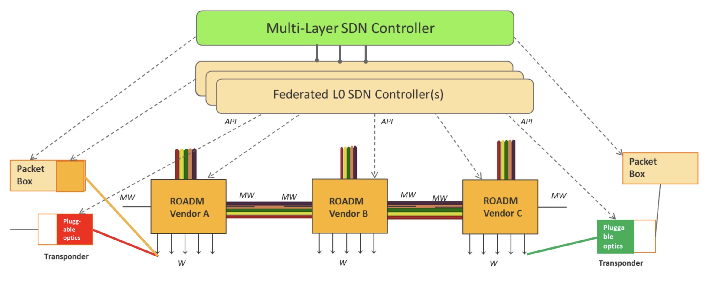
Shown are the various elements included in the disaggregated Open ROADM MSA. Also shown is the hierarchical SDN controller architecture with the federated controllers overseeing the optical layer and the multi-layer controller overseeing the path creation across the layer, from IP to optical. Source: Open ROADM MSA

Meanwhile, the Open ROADM multi-source agreement (MSA) continues to progress, with members working on Release 6.0 of the standard. 

Click to read more ...

Wednesday
Jun292016

FPGAs with 56-gigabit transceivers set for 2017

Xilinx is expected to ship its first FPGAs featuring 56-gigabit transceivers next year. 

The company demonstrated a 56-gigabit transceiver using 4-level pulse-amplitude modulation (PAM-4) at the recent OFC show. The 56-gigabit transceiver, also referred to as a serialiser-deserialiser (serdes), was shown successfully working over backplane specified for 25-gigabit signalling only.

Gilles GarciaXilinx's 56-gigabit serdes is implemented using a 16nm CMOS process node but the first FPGAs featuring the design will be made using a 7nm process. Gilles Garcia says the choice of 7nm CMOS is solely a business decision and not a technical one.

”Optical module [makers] will take another year to make something decent using PAM-4," says Garcia, Xilinx's director marketing and business development, wired communications. "Our 7nm FPGAs will follow very soon afterwards.”

Click to read more ...

Sunday
Jun282015

Altera’s 30 billion transistor FPGA 

  • The Stratix 10 features a routing architecture that doubles overall clock speed and core performance 
  • The programmable family supports the co-packaging of transceiver chips to enable custom FPGAs  
  • The Stratix 10 family supports up to 5.5 million logic elements
  • Enhanced security features stop designs from being copied or tampered with      

Altera has detailed its most powerful FPGA family to date. Two variants of the Stratix 10 family have been announced: 10 FPGAs and 10 system-on-chip (SoC) devices that include a quad-core 64-bit architecture Cortex-A53 ARM processor alongside the programmable logic. The ARM processor can be clocked at up to 1.5 GHz.

The Stratix 10 family is implemented using Intel’s 14nm FinFET process and supports up to 5.5 million logic elements. The largest device in Altera’s 20nm Arria family of FPGAs has 1.15 million logic elements, equating to 6.4 billion transistors. “Extrapolating, this gives a figure of some 30 billion transistors for the Stratix 10,” says Craig Davis, senior product marketing manager at Altera. 


Altera's HyperFlex routing architecture. Shown (pointed to by the blue arrow) are the HyperFlex registers that sit at the junction of the interconnect traces. Also shown are the adaptive logic module blocks. Source: Altera.

Click to read more ...

Sunday
May102015

Optical networking: The next 10 years 

Feature - Part 2: Optical networking R&D

Predicting the future is a foolhardy endeavour, at best one can make educated guesses.

Ioannis Tomkos is better placed than most to comment on the future course of optical networking. Tomkos, a Fellow of the OSA and the IET at the Athens Information Technology Centre (AIT), is involved in several European research projects that are tackling head-on the challenges set to keep optical engineers busy for the next decade.

“We are reaching the total capacity limit of deployed single-mode, single-core fibre,” says Tomkos. “We can’t just scale capacity because there are limits now to the capacity of point-to-point connections.”


Source: Infinera 

The industry consensus is to develop flexible optical networking techniques that make best use of the existing deployed fibre. These techniques include using spectral super-channels, moving to a flexible grid, and introducing ‘sliceable’ transponders whose total capacity can be split and sent to different locations based on the traffic requirements.

Click to read more ...

Wednesday
Apr082015

PMC advances OTN with 400 Gigabit processor

Optical modules for the line-side are moving beyond 100 Gigabits to 200 Gigabit and now 400 Gigabit transmission rates. Such designs are possible thanks to compact photonics designs and coherent DSP-ASICs implemented using advanced CMOS processes. 


An example switching application showing different configurations of the DIGi-G4 OTN processor on the line cards. Source: PMC

For engineers, the advent of higher-speed line-side interfaces sets them new challenges when designing the line cards for optical networking equipment. In particular, the framer silicon that interfaces to the coherent DSP-ASIC, on the far side of the optics, must cope with a doubling and quadrupling of traffic.  

Click to read more ...

Tuesday
Mar312015

Acacia unveils 400 Gigabit coherent transceiver

  • The AC-400 5x7 inch MSA transceiver is a dual-carrier design
  • Modulation formats supported include PM-QPSK, PM-8-QAM and PM-16-QAM
  • Acacia’s DSP-ASIC is a 1.3 billion transistor dual-core chip 

Acacia Communications has unveiled the industry's first flexible rate transceiver in a 5x7-inch MSA form factor that is capable of up to 400 Gigabit transmission rates. The company made the announcement at the OFC show held in Los Angeles. 

Dubbed the AC-400, the transceiver supports 200, 300 and 400 Gigabit rates and includes two silicon photonics chips, each implementing single-carrier optical transmission, and a coherent DSP-ASIC. Acacia designs its own silicon photonics and DSP-ASIC ICs.

Click to read more ...