

Using LED-based parallelism for fast optical interconnects
Avicena Tech has demonstrated what it claims is the world's smallest one terabit optical transceiver. And the company will reveal more about how it is advancing its optical technology for volume production at the upcoming OFC event in San Diego in March.
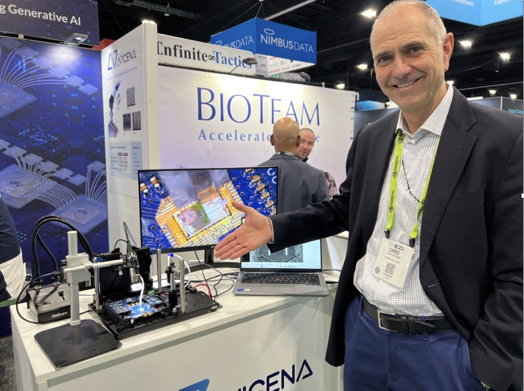 Christoph Pfistner demonstrating the microLED-based 1Tbps interface at Supercomputing 23 in Denver, Colorado.
The interface technology uses compact light emitting diodes (LED). The interface uses an array of these microLEDs that emit light vertically into a bundle of multimode optical fibres.
Avicena demonstrated its 1 terabit-per-second (Tbps) interface at the recent Supercomputing 23 show in Colorado last November. Its interface used 304 LED-based optical channels, each carrying 3.3 gigabit-per-second (Gbps) of data for a total bandwidth of one terabit.
The transceiver design dubbed LightBundle comprises a small 16nm CMOS process chip. Measuring 3mm x 4 mm, the chip hosts the electrical interface and the optical circuitry. These include the microLEDs, each one less that 10 microns in diameter, that emit blue light.
The LEDs are arranged in 2D arrays that are flip-chipped and bonded onto the chip. The photo-detectors are also arranged in an array and connected to the LEDs via the multimode fibres.
"On the electrical side [of the Lightbundle chip], you can put any interface you want," says Christoph Pfistner, vice president of sales and marketing at Avicena. The ASIC uses the Open Compute Project's OpenHBI interface for the electrical interface.
The choice of OpenHBI was due to a hyperscaler customer request. But Avicena plans to use the UCIe chiplet interface for future designs.
Performance metrics
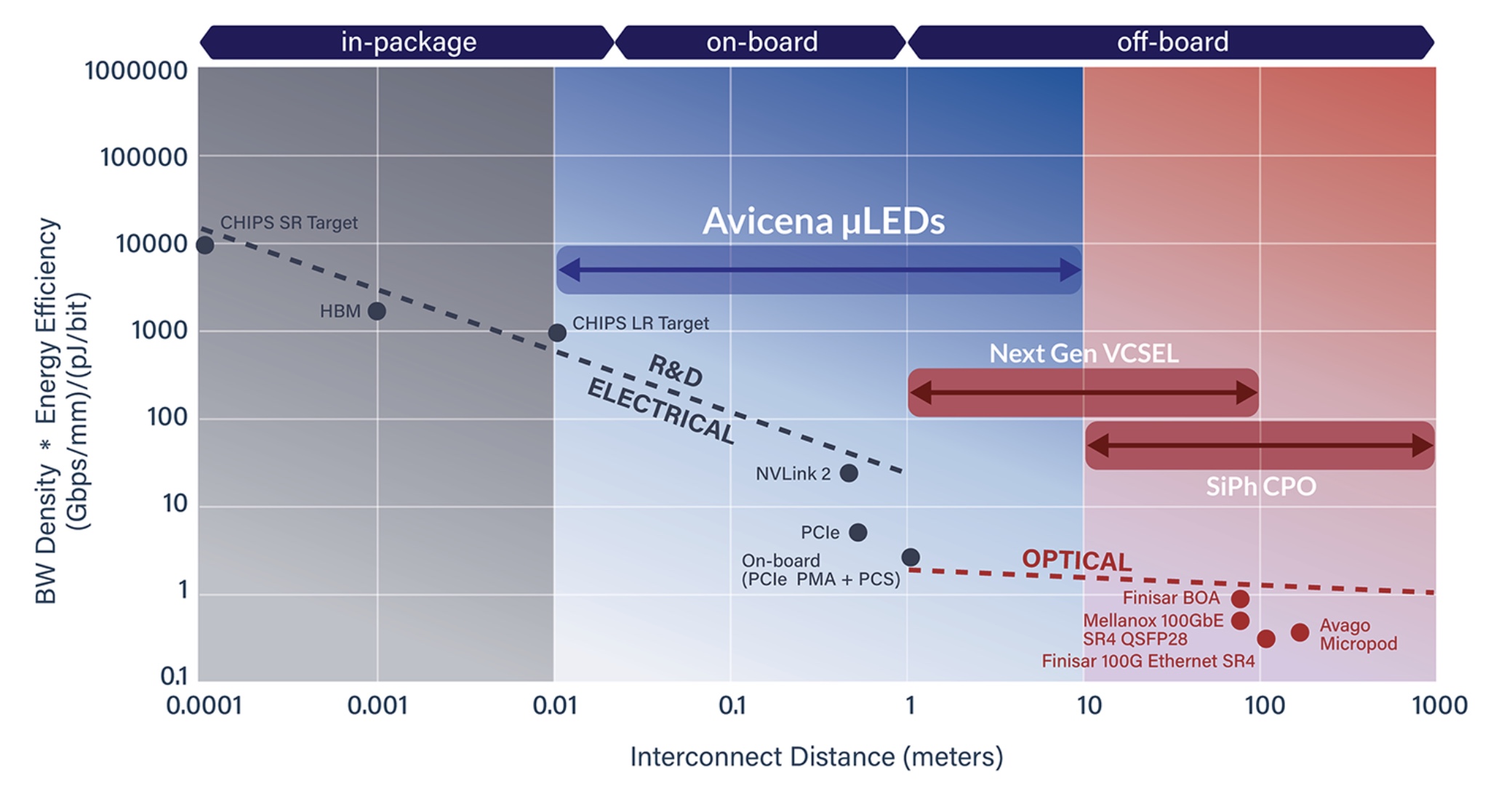
MicroLEDs offer another category of optical interfaces alongside pluggable optical modules, on-board optics, and co-packaged optics (see chart below).
Pfistner stresses that the microLED approach is complementary and does not directly compete with silicon photonics.
 Source: Avicena
The microLEDs and multimode fibre result in a shorter reach interface - up to 10m - whereas silicon photonics interfaces cover a wider span. MicroLED technology is thus ideal for chip-to-chip applications such as interfacing graphics processor units (GPUs) with high-bandwidth memory (HBM). The microLED technology also benefits intra-rack links.
That said, Pfistner is keen to highlight the technology's benefits. First, there is no need for an external laser source, and the link consumes fewer picoJoules-per-bit (pJ/b). Avicena says the channel consumes 1pJ/b and says its roadmap suggests sub-pJ/b interface energy consumption. Silicon photonics interfaces typically consume 3-5pJ/b, although the performance metric should also include the extranal laser source.
Like silicon photonics, the LED-based solution can send significant bandwidth across a small length of the chip's edge, referred to as 'beachfront' density. Pfistner says the company can achieve more than 10Tbps/mm interface densities, with the company's roadmap potentially going to 25Tbps/mm.
Given that this technology is multimode, there is also a relaxed tolerance – a few microns - to coupling the LED light source to the fibre bundle. This is a much more relaxed tolerance than single-mode fibre designs, which require sub-micron precision. More relaxed laser manufacturing tolerances means lower production costs.
The LED-based interface technology can also operate at over 150°C, much higher than traditional lasers. Operating temperatures up to 290°Chave been demonstrated in collaboration with Fred Kish's North Carolina State University (NCSU) group, says Pfistner.
And since the chip supports non-return-to-zero (NRZ) signalling over short-reach spans, it has a latency advantage compared to optical interfaces requiring signal processing and error correction schemes to close links.
Active optical cable
The company's first use of its technology is for an active optical cable product.
At first glance, this is counterintuitive: active optical cables use 50-gigabit or 100-gigabit PAM4 electrical interfaces, whereas Avicena's technology is fed using many electrical interfaces each at lower speed, just several gigabits per second. Accordingly, inside the module at each end of the cable, a gearbox chip is needed to convert the 100Gbps electrical signal into many lower-speed electrical signals before being transmitted over the LED links.
The same applies at the receiver end; the many slow optical signals are recovered and multiplexed from low-speed electrical signals into high-speed 50-gigabit or 100-gigabit PAM4 electrical signals.
Avicena is working with a chip partner to develop a 12nm chip with a gearbox block coupled to its LightBundle chip IP. The design will enable an 800-gigabit Ethernet active optical cable where the chip and optics consume 5W at each end.
The design will be less costly than other optical designs and can compete with 800-gigabit active electrical cables on cost but with a more extended reach. The technology will also scale to 1.6Tbps active optical cables.
High bandwidth memory
Longer term, Avicena is eyeing the HBM opportunity. HBM uses stacked high-speed memory dies, with several HBMs seated around a processor IC. There is an ongoing race to stack more data in the HBM, overall memory for the processor such as GPUs, and faster data access speeds.
However, HBM has several constraints. First, only so many chips can be stacked on each other in part due to heat dissipation issues. The memory chip at the bottom of the stack must dissipate its heat through all the chips above it, and hot HBM stacks require frequent refresh cycles to retain data, which limits usable bandwidth.
One merit of HBM is that it uses a large bus - 1024 electrical channels wide, each at 6.4 Gbps (HBM3). This is ideal for Avicena's microLED optical interface. HBM3E memory uses an even faster interface speed of 9.6Gbps. Meanwhile, HBM4, expected in a couple of years, aims to widen the electrical bus from 1024 to 2048 lanes to keep GPU designs fed with data.
Another issue is the size of the stacks relative to the large ASIC chip, such as a GPU. A finite chip size means only so many HBM can surround the ASIC. Due to space limits, high-end GPUs are limited to six HBMs, three stacks on each side of the chip.
Using an optical interface promises larger-capacity high-bandwidth memory designs where the stacks don't have to be crammed around the ASIC. The memory can be located further away but still be accessible with low latency and energy consumption.
The ASIC-to-HBM interface is thus an important opportunity for short-reach optical interconnects. Moreover, two investors in Avicena are Samsung and Micron, leading memory suppliers.
Avicena's is now focussed on preparing customer demo kits and increasing its yields before it ramps production for the first product, topics it will be discussing at OFC 2024.
 Post a Comment
Reader Comments