

Teramount brings pluggability to co-packaged optics
Hesham Taha, the CEO and co-founder of Teramount, describes the last two years for his company as eventful.
"Many things have happened on many fronts," he says.
Teramount has developed a fibre assembly technology for designs integrating photonics and chips.
 Hesham Taha
The start-up has raised $20 million in funding and has 30 staff. In addition, the company is recruiting staff experienced in manufacturing processes.
"The funding helps to support what we are working on today, which is manufacturing readiness," says Taha.
Taha also notes marketplace changes as when the rising interest in co-packaged caused some companies that had stepped out of silicon photonics to return.
The marketplace moves reflect silicon photonics' changing role. The technology is central for integrated designs such as co-packaged optics, whereas before, it had a more peripheral role when used for pluggable optics.
"This is a big change that requires optical integration with electronics, a change in packaging, and how you assemble fibres," says Taha.
Plugs and bumps
Teramount's technology coupling fibre to silicon photonics chips has two elements: a photonic bump and a photonic plug. The two combined avoid having to bond the fibre to the chip directly.
This is important for two reasons.
First, fibre bonding is an extra manufacturing step that impacts adversely the yield of an expensive chip.
Second, the plug, which is on a separate plane from the chip, working together with the photonic bump, enables the fibres to be detached and serviced, much like pluggable optics.
The photonic plug holds the fibres using a V-groove mechanism and couples them to the silicon photonics chip via the photonic bump, a component manufactured as part of the silicon photonics design.
It is the plug and bump combined that deliver large assembly tolerances. "The large tolerances is what enables the detachability," says Taha.
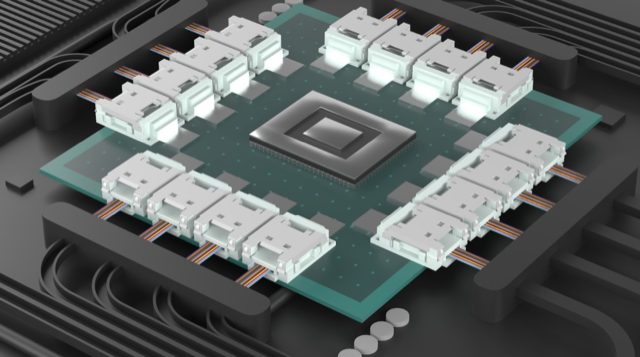 A co-packaged optics design showing the detachable optical interfaces. Source: Teramount
It means a semiconductor company can avoid dealing with fibres and focus on what it does best: designing chips. Foundries and outsourced semiconductor assembly and test (OSAT) companies can handle the wafer-level plug and connect the fibres.
"If the right foundations are set on the silicon photonics wafer, then silicon photonics packaging can become very easy with detachable optics," says Taha.
Surface coupling and edge coupling
Silicon photonics uses two approaches to couple the optical signal from the fibre to a photonics chip.
One, known as surface coupling, uses a grating coupler, while the second uses side coupling.
Grating couplers are wavelength dependent and send the light beam out at a specific angle. Therefore, changing the wavelength affects the angle, complicating the interfacing.
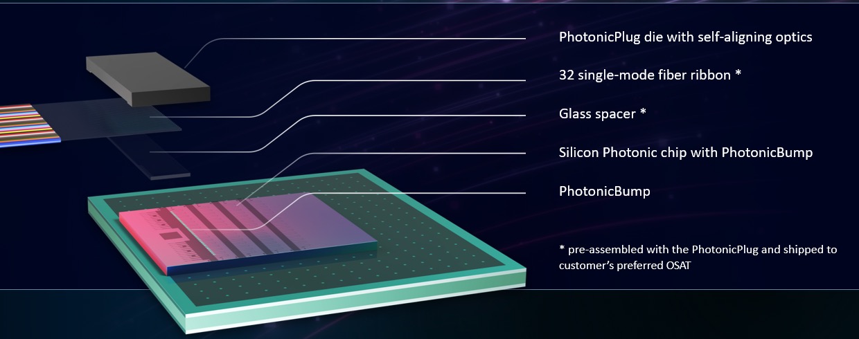 Source: Teramount
As part of the silicon photonics chip design, the photonic bump - effectively a lens - is positioned accurately next to the grating coupler.
In contrast, side coupling collects the beam for the silicon photonic chip's waveguide from the edge of the die. Here, there is no spectral dependency. "You can inject in and out multiple wavelengths," says Taha.
Teramount says side coupling is not viable for the volume manufacturing of silicon photonic designs.
"You cannot connect a fibre from the edge of the die; you have to prepare for a photonic bump before wafer dicing for side coupling," says Taha.
Teramount's design enables light to go to the side of the die, but instead of collecting it from the edge, the photonic bump deflects the beam vertically.
"The photonic bump shifts side coupling into the wideband surface coupling," says Taha.
The photonic bump has two components in the wideband surface coupling case: a wideband deflector and a lens mirror for beam expansion.
The photonic bump and plug combined forms what Teramount calls self-aligning optics. "You have added more complexity in wafer-level manufacturing, but you have relaxed the tolerances in the assembly domain," he says.
The resulting design has assembly tolerances of +/- 30 microns. "Altogether, over 60 microns, you lose only half a dB in misalignment tolerances," he says.
Teramount supports both solutions: surface coupling for a single wavelength and wideband surface coupling for multiple wavelengths. Most customers are working with the wideband solution, says Taha.
The assembly tolerances, wideband surface coupling, and planar separation of the fibres from the die, are what enable fibre detachability, says Taha.
"A technician can manually assemble hundreds of fibres on a co-packaged optics stack," he says.
The fibre assembly process is compatible with semiconductor packaging techniques. No fibre reflow soldering is needed, improving co-packaged optics' yield while enabling the servicing of the fibre assembly for co-packaged optics.
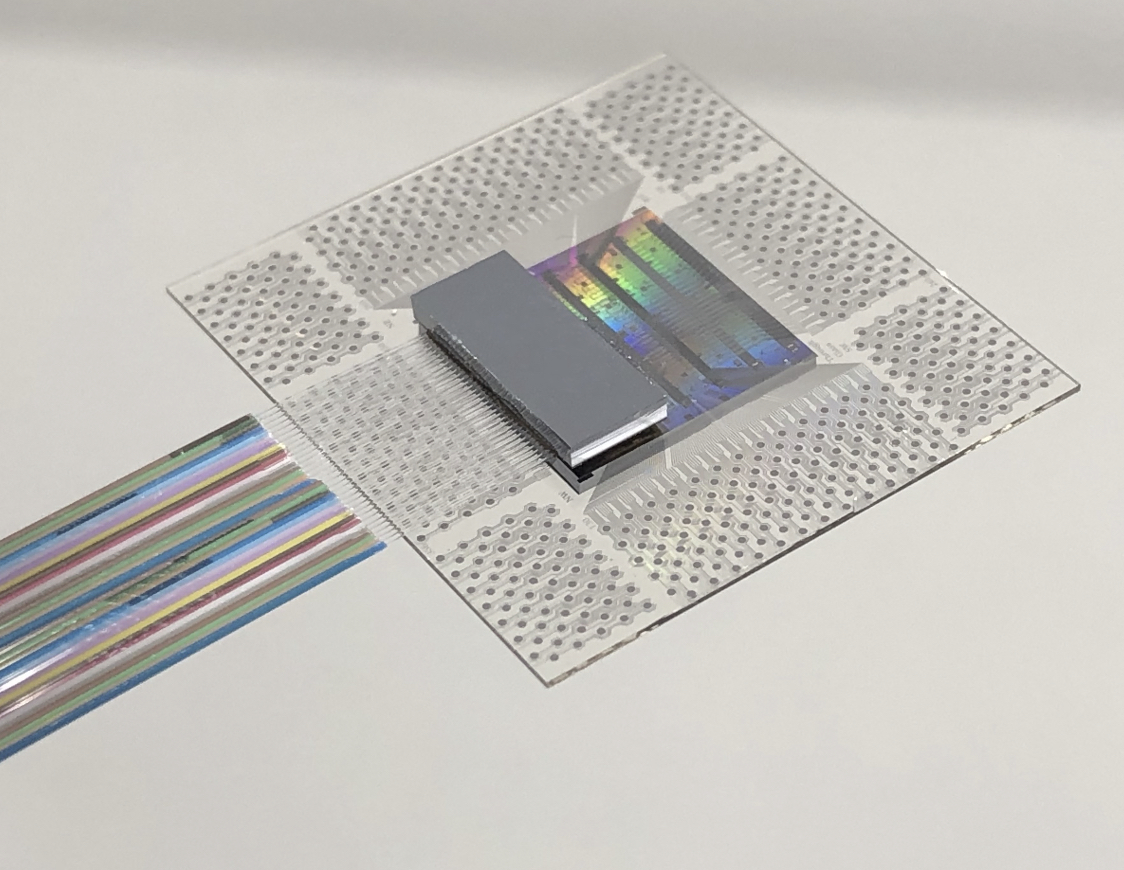 Source: Teramount
Status
Teramount announced in 2022 a collaboration with EV Group, an equipment and process solutions supplier, to tackle wafer-level optics.
Taha says Teramount is working with foundries, OSATs and wafer-level optics manufacturers, such as EV group, to create an ecosystem for its photonic bump and photonic plug technology.
"We want the customer to have the ability to use a foundry to include in their wafer a photonic bump," says Taha. "Once there, a customer can enjoy the photonic plug connector, its relaxed assembly tolerances, and detachable fibre connectivity."
Teramount is also working with vendors in networking and computing, developers of co-packaged optics and optical input-output for processor clusters used for machine learning, respectively.
"We've already sent samples to customers that we are working with, which includes 32 fibres," says Taha.
Teramount intends to announce more collaborations with vendors and wafer-manufacturing suppliers.
 Post a Comment
Reader Comments