Ambitious European project seeks to combine lasers, electronics and photonics, all on one chip
Several companies and research institutes, part of a European project, are developing a silicon photonics process that combines on-chip electronics and lasers. Dubbed Dimension (Directly Modulated Lasers on Silicon), the silicon photonics project is part of the European Commission’s Horizon 2020 research and innovation programme.
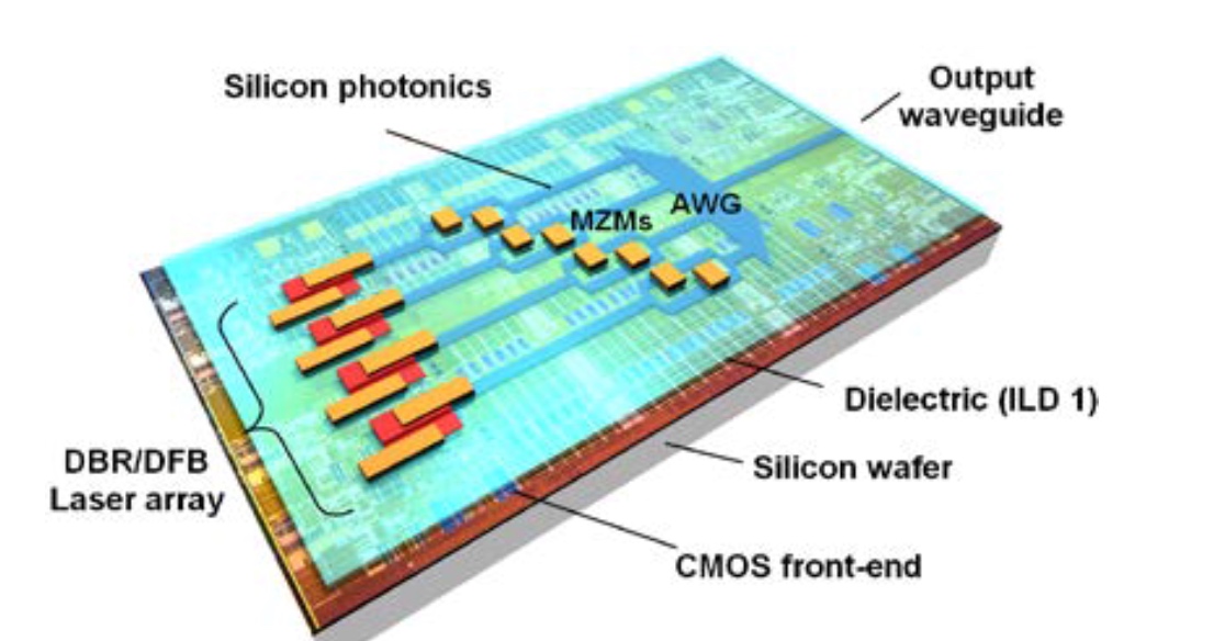 The Dimension process showing the passive photonics, dielectric material, BiCMOS circuitry, and the on-chip lasers and modulators. The indium phosphide material is shown in red. Source: Dimension.
Goal
Silicon photonics has long been seen as a technology having the potential to deliver optical devices at CMOS manufacturing costs. But silicon's key shortfall is that it does not lase. “What we see with today’s solutions is a very low-cost chip with a lot of functionality, which is a great thing, but in addition you need lasers,” says Bert Offrein, principal research staff member and manager of neuromorphic devices and systems at IBM Research, a participant in the Dimension project.
The laser accounts for a relatively large fraction of the total bill of materials of a silicon photonics chip. In turn, connecting the light source to the chip is not trivial and adds to the packaging costs. “In this project, we try to tackle this [laser] issue,” says Offrein.
The project's goal is to develop manufacturing processes that will enable the integration of photonics, including the laser, and electronics, all on one chip. “By fully integrating the laser on the chip, we massively reduce the cost and create additional functionality,” says Offrein.
“This is the true embodiment of what people first pictured as silicon photonics: the combination of optics and electronics on a single chip,” says Lars Zimmermann, team leader, silicon photonics at the Innovations for High Performance Microelectronics (IHP) research institute, another member of Dimension.
Proof-of-concept demonstrators
Dimension is a four-year project that will end in early 2020. Other project participants besides IBM Research and the IHP include ADVA Optical Networking, Opticap and the Athens Information Technology (AIT) research centre. The Dresden University of Technology is overseeing the project.
The project has set itself the goal of producing three proof-of-concept designs using the integrated silicon photonics technology.
One is a 400 Gigabit Ethernet (GbE) transmitter made up of eight 50 gigabit-per-second (Gbps) channels, each comprising a 25 gigabaud directly-modulated laser combined with 4-level pulse amplitude modulation (PAM4). Two variants are planned: a directly modulated version for the 400GbE 2km reach specification, and one with external modulation for the 400GbE 10km reach standard.
Another design is a coherent transmitter for such applications as data centre interconnect, compromising a monolithically integrated narrow-linewidth tunable laser, modulator and driver. The coherent transmitter will have a 10km target reach, will operate at 25Gbps and have a tunable narrow linewidth of under 1MHz.
The third, final demonstrator is a directly-modulated 25-gigabit non-return-to-zero laser using indium phosphide grown directly on the silicon.
By fully integrating the laser on the chip, we massively reduce the cost and create additional functionality
Process details
The silicon photonics manufacturing process involves using a silicon-on-insulator (SOI) wafer to implement the passive photonics functions and the electronics. The electronics supports high-speed analogue driver transistors and a 0.25-micron BiCMOS process used to implement the chip's control logic and control interfaces.
 Bert Offrein
The laser is constructed by first bonding a thin layer of indium phosphide. “It is structured in such a way that it [the III-V material] can be embedded completely in the whole CMOS processing,” says Offrein.
The indium phosphide layer, referred to as a III-V membrane, sits on a thin dielectric layer placed on the SOI wafer. The dielectric material is needed to protect the wafer from contamination by the III-V material and ensure that such a design could be manufactured in a BiCMOS foundry.
Once the thin indium phosphide layer is deposited, the laser can be constructed. The final stages, part of the chip-making back-end process, is the adding of metallisation layers that connect the laser and the electronics, and the circuits to the interface signals.
Growing lasers on silicon
Growing the indium phosphide layer directly on silicon, as will be done for the third demonstrator, is more exploratory. “We want to show there is a path forward on this III-V-on-silicon technology to reduce the cost further,” says Offrein.
 Lars Zimmermann
The challenge growing indium phosphide on silicon is the lattice mismatch that occurs between the two materials which leads to defects.
To tackle the issue, an approach known as confined growth is used. A small ‘seed’ is put on the silicon to act as a growth point for the indium phosphide. A small cavity is created using silica to confine the resulting growth. “The material grows in this glass cavity and the defects grow out and disappear at the edges,” says Offrein. “You then have a very high-quality III-V in this glass and this is the starting point to continue to build the quantum wells that we need.”
One challenge is enlarging the confined growth area. So far, such growth is limited to a micron whereas the length of a laser can be 500 microns typically. And once the laser is built, there remain the issues of laser reliability and temperature stability. “We will see challenges but we are not there yet,” says Offrein.
This is the true embodiment of what people first pictured as silicon photonics: the combination of optics and electronics on a single chip
Status
Dimension is tackling designs for communications but such on-chip lasers will also be useful for a range of applications such as optical sensing, says Offrein.
The project is coming to the end of its first year. Its members are creating the basic building blocks needed to realise the lasers on the silicon wafer. IBM has demonstrated the basic functionality by bonding indium phosphide to its own passive silicon photonics technology. “We have also realised the first lasers - not yet electrically pumped but optically pumped,” says Offrein. The performance of these lasers is now being characterised.
All the processes needed to pump the lasers electrically are now in place and the goal is to build complete laser structures by March 2017.
IBM is also working with IHP to see what is required to implement the technology using IHP’s own silicon photonics process. IHP is currently testing IBM’s wafers regarding any contamination issues before testing the integration process.
ADVA Optical Networking would not be on board if they were not expecting eventually to have such technology available for their products
Exploitation
The European Commission has a long history of programmes backing leading-edge research. However, Europe's track record of exploiting such research to achieve market-leading companies and products has been limited.
The European Commission staff involved in planning the Horizon 2020 projects have been far more active in ensuring that these projects are exploited, says Zimmermann. "ADVA Optical Networking would not be on board if they were not expecting eventually to have such technology available for their products," he adds.
If Dimension proves successful, IHP could make available the integrated silicon photonics process to companies to implement their opto-electronic integrated circuit designs.
IBM, while no longer a semiconductor manufacturer, would also be keen for the technology to be transferred to large foundries such as STMicroelectronics and GlobalFoundries. “That way we could purchase the technology and apply it in our own systems,” says Offrein.
Article amended on Nov 29th. Added details about the proof-of-concept demonstrators.