counter for iweb
Website
Silicon Photonics

Published book, click here

Entries in Xilinx (10)

Wednesday
Jul292020

Xilinx’s Versal Premium ready for the 800-gigabit era

When Xilinx was created in 1984, the founders banked on programmable logic becoming ever more attractive due to Moore’s law.

Making logic programmable requires extra transistors so Xilinx needed them to become cheaper and more plentiful, something Moore’s law has delivered, like clockwork, over decades.

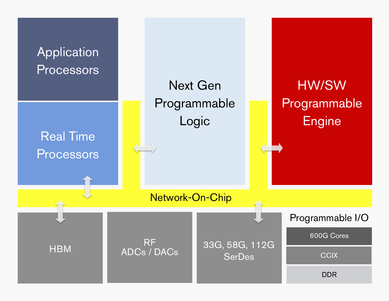
Kirk SabanSince then, Xilinx’s field-programmable gate array (FPGA) devices have advanced considerably.

Indeed, Xilinx’s latest programmable logic family, the Versal Premium, is no longer referred to as an FPGA but as an adaptive compute accelerator platform (ACAP).

The Versal Premium series of chips, to be implemented using TSMC’s 7nm CMOS process, was unveiled for the OFC 2020 show. The Premium series will have seven chips with the largest, the VP1802, having 50 billion transistors.

First devices will ship in the second half of 2021.

Click to read more ...

Tuesday
Jul242018

Xilinx delivers 58G serdes and showcases a 112G test chip

In the first of two articles, electrical input-output developments are discussed, focussing on Xilinx’s serialiser-deserialiser (serdes) work for its programmable logic chips. In Part 2, the IMEC nanoelectronics R&D centre’s latest silicon photonics work to enable optical I/O for chips is detailed.

Part 1: Electrical I/O

Processor and memory chips continue to scale exponentially. The electrical input-output (I/O) used to move data on and off such chips scales less well. Electrical interfaces are now transitioning from 28 gigabit-per-second (Gbps) to 56Gbps and work is already advanced to double the rate again to 112Gbps. But the question as to when electrical interfaces will reach their practical limit continues to be debated. 

Gilles Garcia“Some two years ago, talking to the serdes community, they were seeing 100 gigabits as the first potential wall,” says Gilles Garcia, communications business lead at Xilinx. “In two years, a lot of work has happened and we can now demonstrate 112 gigabits [electrical interfaces].”

The challenge of moving to higher-speed serdes is that the reach shortens with each doubling of speed. The need to move greater amounts of data on- and off-chip also has power-consumption implications, especially with the extra circuitry needed when moving from non-return-to-zero signalling to the more complex 4-level pulse-amplitude modulation (PAM-4) scheme.  

PAM-4 is already used for 56-gigabit electrical I/O for such applications as 400 Gigabit Ethernet optical modules and by the leading edge 12.8-terabit capacity switch chips. Having 112-gigabit serdes at least ensures one further generation of switch chips and optical modules but what comes after that is still to be determined. Even if more can be squeezed out of copper, the trace lengths will shorten and optics will continue to get closer to the chip. 

Click to read more ...

Wednesday
Mar212018

Xilinx unveils a new class of compute IC 

Programmable device company Xilinx has outlined an architecture that it claims represents a new class of computing chip.

The silicon architecture has been four years in the making, involved 1,500 engineers and cost over $1 billion in R&D investment.

ACAP's functional blocks. Source: Xilinx

Dubbed the adaptive compute acceleration platform (ACAP), the first device will be fabricated using TSMC’s state-of-the-art 7nm CMOS process and will tape out later this year. The largest ACAP devices will use as many as 50 billion transistors.

“Based on the limited information from Xilinx, it is difficult to say what ACAP is, much less whether it creates a new product category,” says Linley Gwennap, principal analyst at The Linley Group.

That said, Gwennap believes the next-generation Xilinx products are far more than simply moving its FPGA technology to a 7nm CMOS. “The company has clearly put significant effort into improving the capabilities of these products to address 5G wireless, machine learning (AI), and other advanced applications,” says Gwennap.

Click to read more ...

Wednesday
Jun292016

FPGAs with 56-gigabit transceivers set for 2017

Xilinx is expected to ship its first FPGAs featuring 56-gigabit transceivers next year. 

The company demonstrated a 56-gigabit transceiver using 4-level pulse-amplitude modulation (PAM-4) at the recent OFC show. The 56-gigabit transceiver, also referred to as a serialiser-deserialiser (serdes), was shown successfully working over backplane specified for 25-gigabit signalling only.

Gilles GarciaXilinx's 56-gigabit serdes is implemented using a 16nm CMOS process node but the first FPGAs featuring the design will be made using a 7nm process. Gilles Garcia says the choice of 7nm CMOS is solely a business decision and not a technical one.

”Optical module [makers] will take another year to make something decent using PAM-4," says Garcia, Xilinx's director marketing and business development, wired communications. "Our 7nm FPGAs will follow very soon afterwards.”

Click to read more ...

Wednesday
Dec172014

OpenCL and the reconfigurable data centre

Part 3: General purpose data centres

Xilinx's adoption of the Open Computing Language (OpenCL) as part of its SDAccel development tool is important, not just for FPGAs but also for the computational capabilities of the data centre.

The FPGA vendor is promoting its chips as server co-processors to tackle complex processing tasks such as image searches, encryption, and custom computation.   

Search-engine specialists such as Baidu and Microsoft have seen a greater amount of traffic for image and video searches in the last two years, says Loring Wirbel, senior analyst at market research firm, The Linley Group: "All of a sudden they are seeing that these accelerator cards as being necessary for general-purpose data centres."

Click to read more ...

Thursday
Dec112014

What role FPGA server co-processors for virtual routing?

Part 2:  Accelerating virtual routing functions using FPGAs

IP routing specialists have announced first virtual edge router products that run on servers. These include Alcatel-Lucent with its Virtualized Service Router and Juniper with its vMX. Gazettabyte asked Alcatel-Lucent's Steve Vogelsang about the impact FPGA accelerator cards could have on IP routing.


Steve Vogelsang, IP routing and transport CTO, Alcatel-Lucent

The co-processor cards in servers could become interesting for software-defined networking (SDN) and network function virtualisation (NFV).

The main challenge is that we require that our virtualised network functions (vNFs) and SDN data plane can run on any cloud infrastructure; we can’t assume that any specific accelerator card is installed. That makes it a challenge.

Click to read more ...

Wednesday
Dec102014

FPGAs embrace data centre co-processing role

Part 1: Xilinx's SDAccel development tool


The PCIe accelerator card has a power budget of 25W. Hyper data centres can host hundreds of thousands of servers whereas other industries with more specialist computation requirements use far fewers servers. As such, they can afford a higher power budget per card. Source: Xilinx

Xilinx has developed a software-design environment that simplifies the use of an FPGA as a co-processor alongside the server's x86 instruction set microprocessor.

Dubbed SDAccel, the development environment enables a software engineer to write applications using OpenCL, C or the C++ programming language running on servers in the data centre.   

Click to read more ...