Part 2: Co-packaged optics: fibre-attach
Hesham Taha recently returned from a trip to the US to meet with leading vendors and players serving the silicon photonics industry.
 “It is important to continue probing the industry,” says Taha, the CEO of start-up Teramount.
Teramount specialises in fibre assembly technology: coupling fibre to silicon photonics chips.
Taha is now back in the US, this time to unveil Teramount’s latest product at this week’s OFC show being held in San Diego. The company is detailing a new version of its fibre assembly technology, dubbed Teraverse-XD, that doubles the density of fibres connected to a silicon photonics chip.
Teramount is also announcing it is working with GlobalFoundries, a leading silicon-photonics foundry.
Connecting fibre to a silicon photonics device for a pluggable optical module is straightforward. However, attaching fibre to an optical engine for co-packaged optics is challenging. The coupling must be compact and scale to enable even denser connections in future. This is especially true with the co-packaging of future 100-terabit and 200-terabit Ethernet switch chips.
“If I were to describe the last year, it would be aligning our [Teramount] activities to the industry's evolving needs,” says Taha. “A key part of those needs is being driven by optical activities for AI applications.”
Edge versus surface coupling
Companies are pursuing two main approaches to connecting fibre to a silicon photonics device: surface and edge (side) coupling.
Surface coupling - or its academic term, off-plane coupling - deflects light vertically, away from the chip’s surface. In contrast, edge (in-plane) or side coupling sends the optical waveguide’s light straight through to the fibre at the chip’s edge.
A silicon-photonics grating coupler is used for surface coupling, glancing the light away from the chip’s plane. However, the grating coupler is wavelength-dependent such that the angle of the defection varies with the light.
In contrast, side coupling is wideband. “You can carry multiple wavelengths on each channel,” says Taha. However, side coupling has limited interfacing space, referred to as ‘shoreline density’.
Side coupling is also more complicated to manufacture in volume. Directly bonding the fibre to the chip involves adhesive, and the fibres get in the way of reflow soldering. “It [side coupling] is doable for transceivers, but to make co-packaged optics, side coupling becomes complicated,” says Taha.
Teramount’s approach
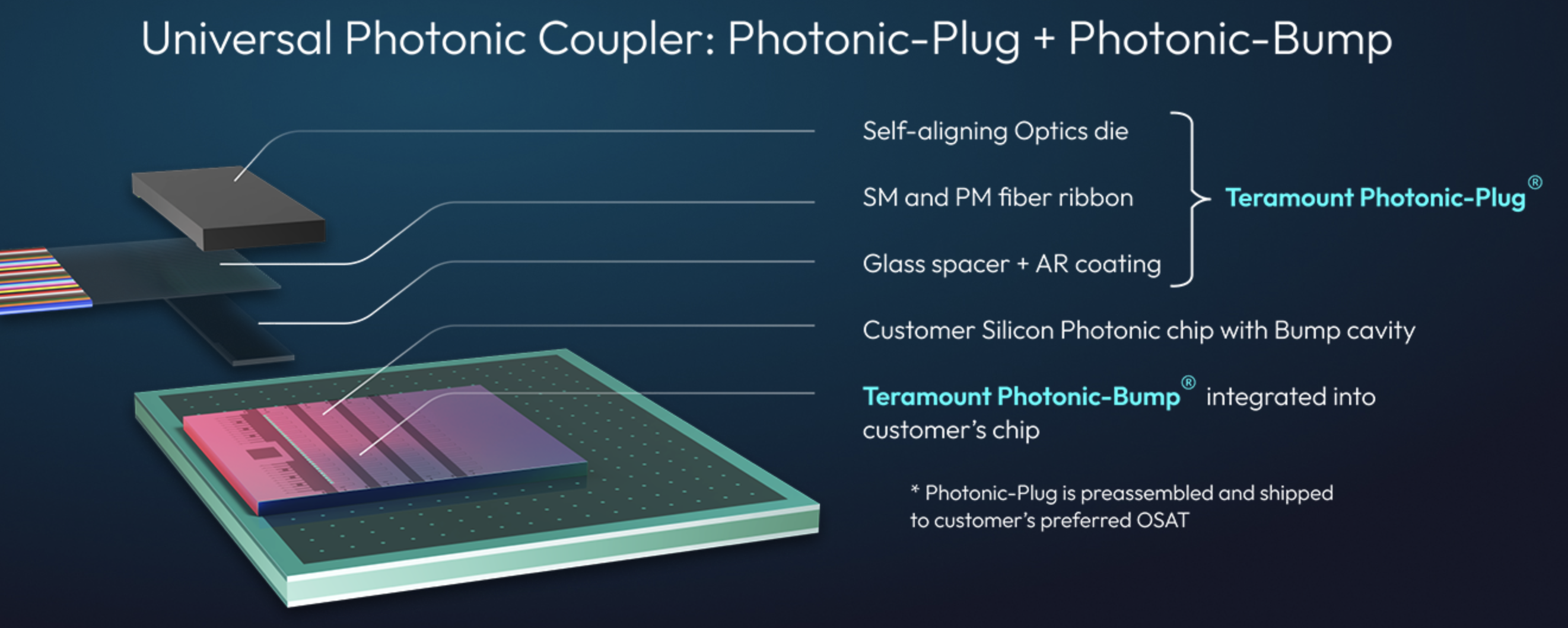
Teramount’s approach couples the fibre to the silicon photonics chip using two components: a photonic plug and a photonic bump.
The photonic plug holds the fibres and couples them to the silicon photonics chip via the photonic bump, a component made during the silicon photonics wafer processing. The photonic bump consists of two elements: a wideband deflector and a lens mirror for beam expansion. Expanding the light beam enables much larger assembly tolerances: +/- 30 microns. And across this 60-micron window, only half a dB is lost in misalignment tolerances.
The resulting wafer-level manufacturing may be more complicated, says Taha, but the benefit is relaxed tolerances in the assembly, wide-band surface coupling, and when testing the wafer and the die.
The photonic bump-and-plug combination also enable detachable optics for co-packaged optics designs. This benefits manufacturing and is wanted for co-packaged optics.
Teraverse and Teraverse-XD
There is a clear demarcation between the optics and the switch chip when using pluggables in the data centre. In contrast, co-packaged optics is a system with the optics embedded alongside the chip. A vendor may work with multiple companies to make co-packaged optics, but one product results, with the chip and optical engined co-packaged.
Teramount’s Teraverse solution, using the plug-and-bump combination, brings pluggability to co-packaged optics. The fibres can be attached and detached from the optical engines. “It’s very important to keep that level of pluggability for co-packaged optics,” says Taha.
The approach also benefits manufacturing yield and testing. Separating the fibres from the package protects the fibres during reflow soldering. “Ideally, you want the fibre connected at the last stage and still maintain high level of testability during the packaging process,” says Taha.
Detachable fibre also brings serviceability to co-packaged optics, benefitting for data centre operators.
Teraverse, Teramount’s detachable fiber-to-chip interface, supports single-mode fiber with 125-micron diameter at a 127-micron pitch separation.
 How to scale fibre count; note the two rows of photonic bumps shown. Source: Teramount
Teraverse-XD, announced for OFC, is a follow-on that doubles the fibre density to achieve a near 64-micron pitch. Here, fibres are placed on top of each other, scaling in the Z-dimension. The approach is like how rods or pipes are stored, with the second row of fibres staggered, sitting in the valleys between adjacent fibers in the lower row.
Two rows of photonic bumps are used to couple the light to each row of fibres (see image above). “It’s very important to keep the same real-estate but to have twice the number of fibres,” says Taha.
Future scaling is possible by adding more rows of fibres or by adopting fibres with a smaller pitch.
Teramount’s technology also supports both edge coupling and surface coupling. “We are agnostic,” says Taha. If a co-packaged optics or optical engine vendor wants to use side coupling, it can use the bump-and-plug combination. The bump deflects the beam upwards to the plug packaging which takes the fibres and sends them out horizontally. “We are converting edge coupling to wideband surface coupling,” says Taha. “You don't need to sacrifice bandwidth to do surface coupling.”
If the vendor wishes to use a grating coupler, Teramount’s bump-and-plug supports that, too, enabling detachable fibering. But here, only the bump’s expanding mirror is used. "For the wideband surface coupling cased, the bump uses two components: the deflector and the expanding mirror," says Taha.
Both cases are supported by what Teramount refers to as its Universal Photonic Coupler, shown.
 Source: Teramount
Market expectations
Despite being discussed for over a decade, Taha is not surprised that data centre operators have yet to adopt co-packaged optics.
He points out that hyperscalers only want to use co-packaged optics for Ethernet switches once the technology is more mature. They can also keep using a proven alternative: pluggable modules, that continue to advance.
"Hyperscalers are not against the technology, but it is not mature enough," says Taha. Hyperscalers and systems vendors also want an established supply chain and not proprietary solutions.
To date, Broadcom's first co-packaged optics switch solution at 25.6-terabit was adopted by Tencent. Broadcom has announced for OFC that it is now delivering its latest 51.2-terabit Bailly co-packaged optics design, backed by ByteDance.
"AI is a different story," says Taha. "This is the tipping point for a leading vendor to start taking seriously co-packaged optics."
The advantage of co-packaged optics here is that it accommodates the reach - radix -as well as power savings and improved latency.
Taha expects initial volumes of co-packaged optics sales in 2026.