Near package optics has emerged as companies have encountered the complexities of co-packaged optics. It should not be viewed as an alternative to co-packaged optics but rather a pragmatic approach for its implementation.
Co-packaged optics will be one of several hot topics at the upcoming OFC show in March.
Placing optics next to silicon is seen as the only way to meet the future input-output (I/O) requirements of ICs such as Ethernet switches and high-end processors.
 Brad Booth
For now, pluggable optics do the job of routing traffic between Ethernet switch chips in the data centre. The pluggable modules sit on the switch platform’s front panel at the edge of the printed circuit board (PCB) hosting the switch chip.
But with switch silicon capacity doubling every two years, engineers are being challenged to get data into and out of the chip while ensuring power consumption does not rise.
One way to boost I/O and reduce power is to use on-board optics, bringing the optics onto the PCB nearer the switch chip to shorten the electrical traces linking the two.
The Consortium of On-Board Optics (COBO), set up in 2015, has developed specifications to ensure interoperability between on-board optics products from different vendors.
However, the industry has favoured a shorter still link distance, coupling the optics and ASIC in one package. Such co-packaging is tricky which explains why yet another approach has emerged: near package optics.
I/O bottleneck
“Everyone is looking for tighter and tighter integration between a switch ASIC, or ‘XPU’ chip, and the optics,” says Brad Booth, president at COBO and principal engineer, Azure hardware architecture at Microsoft. XPU is the generic term for an IC such as a CPU, a graphics processing unit (GPU) or even a data processing unit (DPU).
What kick-started interest in co-packaged optics was the desire to reduce power consumption and cost, says Booth. These remain important considerations but the biggest concern is getting sufficient bandwidth on and off these chips.
“The volume of high-speed signalling is constrained by the beachfront available to us,” he says.
Booth cites the example of a 16-lane PCI Express bus that requires 64 electrical traces for data alone, not including the power and ground signalling. “I can do that with two fibres,” says Booth.
Near package optics
With co-packaged optics, the switch chip is typically surrounded by 16 optical modules, all placed on an organic substrate (see diagram below).
 Nhat Nguyen
“Another name for it is a multi-chip module,” says Nhat Nguyen, senior director, solutions architecture at optical I/O specialist, Ayar Labs.
A 25.6-terabit Ethernet switch chip requires 16, 1.6 terabits-per-second (1.6Tbps) optical modules while upcoming 51.2-terabit switch chips will use 3.2Tbps modules.
“The issue is that the multi-chip module can only be so large,” says Nguyen. “It is challenging with today’s technology to surround the 51.2-terabit ASIC with 16 optical modules.”
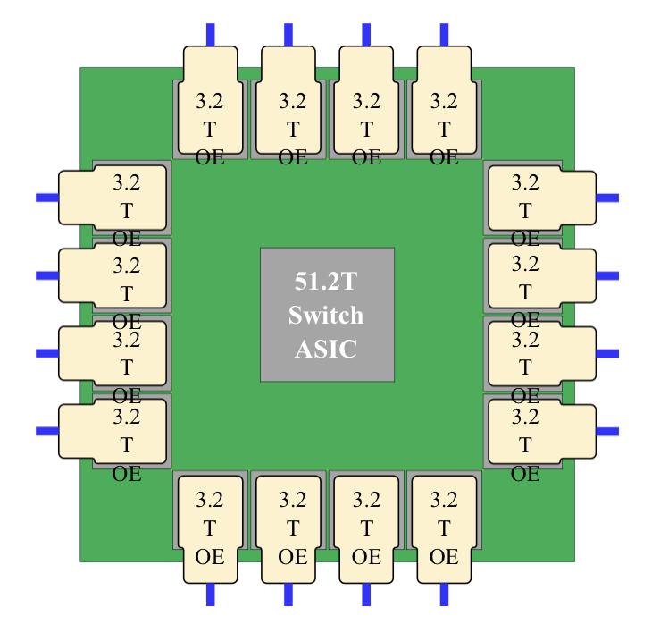 A 51.2-terabit Ethernet switch chip surrounded by 16, 3.2Tbps optical modules. Source: OIF.
Near package optics tackles this by using a high-performance PCB substrate - an interposer - that sits on the host board, in contrast to co-packaged optics where the modules surround the chip on a multi-chip module substrate.
The near package optics’ interposer is more spacious, making the signal routing between the chip and optical modules easier while still meeting signal integrity requirements. Using the interposer means the whole PCB doesn’t need upgrading which would be extremely costly.
Some co-packaged optics design will use components from multiple suppliers. One concern is how to service a failed optical engine when testing the design before deployment. “That is one reason why a connector-based solution is being proposed,” says Booth. “And that also impacts the size of the substrate.”
 Nathan Tracy
A larger substrate is also needed to support both electrical and optical interfaces from the switch chip.
Platforms will not become all-optical immediately and direct-attached copper cabling will continue to be used in the data centre. However, the issue with electrical signalling, as mentioned, is it needs more space than fibre.
“We are in a transitional phase: we are not 100 per cent optics, we are not 100 per cent electrical anymore,” says Booth. “How do you make that transition and still build these systems?”
Perspectives
Ayar Labs views near package optics as akin to COBO.
“It’s an attempt to bring COBO much closer to the ASIC,” says Hugo Saleh, senior vice president of commercial operations and managing director of Ayar Labs U.K.
However, COBO’s president, Booth, stresses that near package optics is different from COBO’s on-board optics work.
“The big difference is that COBO uses a PCB motherboard to do the connection whereas near package optics uses a substrate,” he says. “It is closer than where COBO can go.”
It means that with near package optics, there is no high-speed data bandwidth going through the PCB.
Booth says near package optics came about once it became obvious that the latest 51.2-terabit designs - the silicon, optics and the interfaces between them - cannot fit on even the largest organic substrates.
“It was beyond the current manufacturing capabilities,” says Booth. “That was the feedback that came back to Microsoft and Facebook (Meta) as part of our Joint Development Foundation.”
Near package optics is thus a pragmatic solution to an engineering challenge, says Booth. The larger substrate remains a form of co-packaging but it has been given a distinct name to highlight that it is different to the early-version approach.
Nathan Tracy, TE Connectivity and the OIF’s vice president of marketing, admits he is frustrated that the industry is using two terms since co-packaged optics and near package optics achieve the same thing. “It’s just a slight difference in implementation,” says Tracy.
The OIF is an industry forum studying the applications and technology issues of co-packaging and this month published its framework Implementation Agreement (IA) document.
COBO is another organisation working on specifications for co-packaged optics, focussing on connectivity issues.
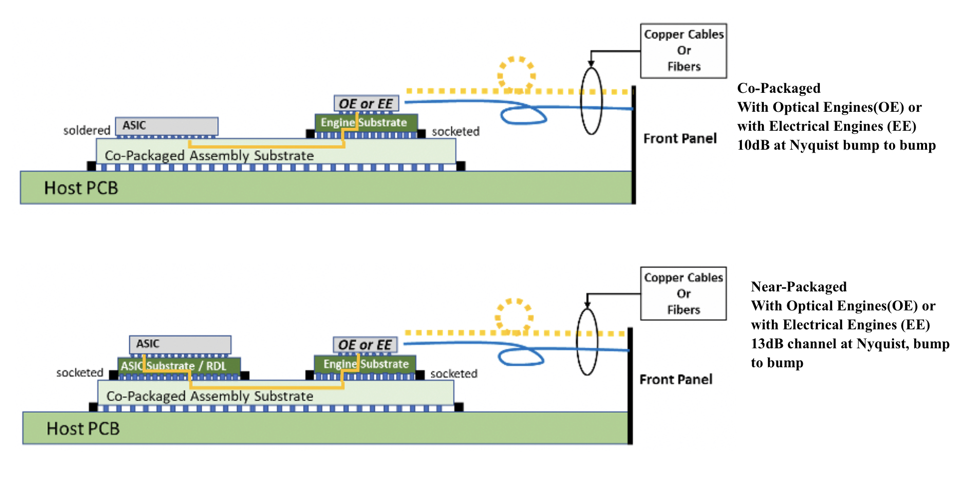 The two design approaches: co-packaged optics and near package optics. Source: OIF.
Technical differences
Ayar Labs highlights the power penalty using near package optics due to its use of longer channel lengths.
For near package optics, lengths between the ASIC and optics can be up to 150mm with the channel loss constrained to 13dB. This is why the OIF is developing the XSR+ electrical interface, to expand the XSR’s reach for near package optics.
In contrast, co-packaged optics confines the modules and host ASIC to 50mm of each other. “The channel loss here is limited to 10dB,” says Nguyen. Co-packaged optics has a lower power consumption because of the shorter spans and 3dB saving.
Ayar Labs highlights its optical engine technology, the TeraPHY chiplet that combines silicon photonics and electronics in one die. The optical module surrounding the ASIC in a co-packaged design typically comprises three chips: the DSP, electrical interface and photonics.
“We can place the chiplet very close to the ASIC,” says Nguyen. The distance between the ASIC and the chiplet can be as close as 3-5mm. Whether on the same interposer Ayar Labs refers to such a design using athird term: in-package optics.
Ayar Labs says its chiplet can also be used for optical modules as part of a co-packaged design.
The very short distances using the chiplet result in a power efficiency of 5pJ/bit whereas that of an optical module is 15pJ/bit. Using TeraPHY for an optical module co-packaged design, the power efficiency is some 7.5pJ/bit, half that of a 3-chip module.
A 3-5mm distance also reduces the latency while the bandwidth density of the chiplet, measured in Gigabit/s/mm, is higher than the optical module.
Co-existence
Booth refers to near package optics as ‘CPO Gen-1’, the first generation of co-packaged optics.
“In essence, you have got to use technologies you have in hand to be able to build something,” says Booth. “Especially in the timeline that we want to demonstrate the technology.”
Is Microsoft backing near package optics?
“We are definitely saying yes if this is what it takes to get the first level of specifications developed,” says Booth.
 Hugo Saleh
But that does not mean the first products will be exclusively near package optics.
“Both will be available and around the same time,” says Booth. “There will be near packaged optics solutions that will be multi-vendor and there will be more vertically-integrated designs; like Broadcom, Intel and others can do.”
From an end-user perspective, a multi-vendor capability is desirable, says Booth.
Ayar Labs’ Saleh sees two developing paths.
The first is optical I/O to connect chips in a mesh or as part of memory semantic designs used for high-performance computing and machine learning. Here, the highest bandwidth and lowest power are key design goals.
Ayar Labs has just announced a strategic partnership with high performance computing leader, HPE, to design future silicon photonics solutions for HPE’s Slingshot interconnect that is used for upcoming Exascale supercomputers and also in the data centre.
The second path concerns Ethernet switch chips and here Saleh expects both solutions to co-exist: near package optics will be an interim solution with co-packaged optics dominating longer term. “This will move more slowly as there needs to be interoperability and a wide set of suppliers,” says Saleh.
Booth expects continual design improvements to co-packaged optics. Further out, 2.5D and 3D chip packaging techniques, where silicon is stacked vertically, to be used as part of co-packaged optics designs, he says.