Ranovus says two of its lead customers will deploy co-packaged optics next year.
They will deploy 25.6-terabit Ethernet switch chips but these will be proof-of-concept designs rather than volume deployments.
 Hamid ArabzadehThe deployments will be used to assess the software and gain experience with their maintenance including replacing optics if needed.
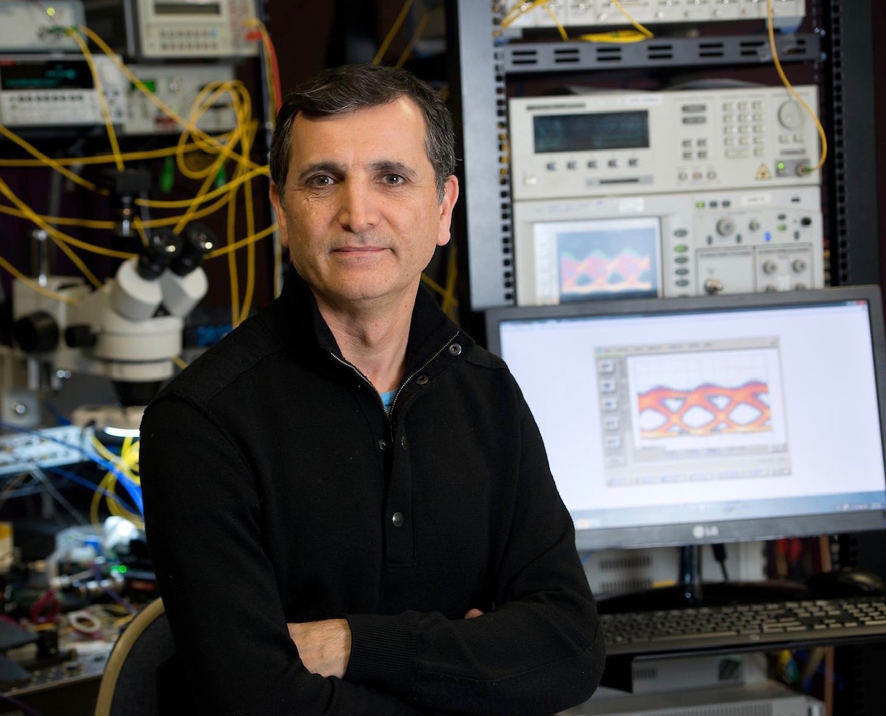
“I do think 2024 is going to be the volume year,” says Hamid Arabzadeh, CEO of Ranovus, who expects to announce the customers before the year-end.
Applications
Ranovus is focussed on the emerging integrated optical input-output (I/O) market for Ethernet switches and disaggregated server designs.
A disaggregated server untangles the compute, memory and storage elements found on a server card and pools them separately. This enables a CPU or compute node to access far more memory. It also means each of the server elements can be upgraded independently.
Pooling the memory suits artificial intelligence (AI)/ machine learning applications that process huge data sets. Such applications also require considerable computing.
For machine learning applications, graphic processing unit (GPU) chips are tightly coupled in clusters. But it is a challenge to continually grow the number of GPUs in a cluster and support inter-cluster communications using eletrical interfaces.
Data centre operators want processing performance that scales linearly as more GPUs are adding to a cluster and more clusters are used. This requires longer-reach, high-bandwidth, low-latency links. Limiting the power consumption of such links is also key.
Such system design challenges explain the industry’s interest in adding optical I/O to high-end processors like GPUs. The same applies to Ethernet switch-chips that are doubling in capacity every two years. Moving from electrical to optical interfaces promises longer, energy efficient (measured in pJ/bit), low-latency links.
For Ethernet switch designs, the optical I/O end-point bandwidth needed is at least 3.2 terabits per second (Tbps), says Arabzadeh, whereas for AI it is 0.5-1Tbps.
Odin optical engine
Ranovus recently expanded its optical interconnect portfolio by developing an Odin design that doesn’t need an accompanying retimer chip.
The optical engine combines CMOS and silicon photonics circuits in a monolithic chip, resulting in a smaller, cheaper and power-efficient design.
This second-generation Odin means Ranovus can now offer digital and analogue drive options for co-packaged optics and address more cost-conscious applications such as chip interconnect in servers.
Arabzadeh says its first Odin design that uses a retimer chip helped secure its lead customers.
“We have two lead customers where we are doing the co-packaging of their [switch] chips operating at 100-gigabit PAM-4,” he says. “And we also have an AI customer, where their chip talks PCI Express 5.0 (PCIe 5.0) to our Odin.”
Ranovus first unveiled its Odin-8 800-gigabit design at OFC 2020 and demonstrated it sending eight 100 gigabit PAM-4 (4-level pulse-amplitude modulation) signals, each on a separate fibre.
The design includes a digital retimer IC which takes the OIF-standard extra short reach (XSR) signal - for example, from a switch chip - and recreates (retimes) the PAM-4 signal before forwarding it to Ranovus’ chip. Such a configuration is referred to as a digital-drive design.
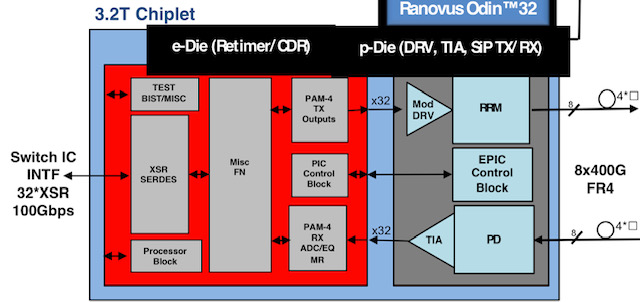 A diagram showing the Odin 32, with Ranovus' chip alongside the retimer IC. Source: Ranovus
“This retimer is not a chip we do and it is expensive,” says Arabzadeh. “It also consumes half the power of the [Odin] chiplet design.”
Ranovus also detailed over a year ago its Odin-32 design that supports four wavelengths per fibre for a total bandwidth of 3.2Tbps.
Since then, Ranovus has developed its Odin-8 for use in an 800-gigabit DR8 optical module. The module will sample and be in the hands of customers for testing in the coming quarter.
The Odin-based 800G-DR8 optical module has a power consumption of 13W; 4W less than rival designs, says Arabzadeh, adding that the optical engine is cost-effective at 400 gigabits, even when using half its capacity.
ODIN version 2.0
The latest monolithic chip is an analogue-drive design. It features radio frequency (RF) drivers, trans-impedance amplifiers (TIAs), silicon photonics transmitters and receivers, and control logic to oversee the components.
The chip does away with clock data recovery (CDR) while integrating the TIAs on-chip. This reduces system costs. “We have the first TIA at 100 gigabits in CMOS,” says Arabzadeh.
To work without the retimer, the monolithic chip is placed much closer to the driving ASIC, with both sharing a common substrate. “It works because it is parked right next to the other chip,” says Arabzadeh.
Ranovus uses a software model of a vendor’s ASIC’s serialiser/ deserialiser (serdes) to ensure the serdes will drive its analogue input.
Being an analogue drive, it is bit-rate and protocol agnostic. “This allows us to get customers beyond the Ethernet market,” says Arabzadeh. These include 100-gigabit PAM-4 signals and the PCIe 5.0 protocol, as mentioned.
For machine learning applications, a proprietary protocol can be used between the end points. NVLink, a serial multi-lane communications link developed by Nvidia, is one such protocol.
Arabzadeh says Ranovus has achieved 1 terabit-per-mm in pitch interface densities: “The stuff we have got involved in with folks in machine learning and AI dwarfs the Ethernet market.”
Laser source
Ranovus’ co-packaged designs use an external laser source. But the company has patented technlogy that allows lasers to be attached directly to the monolithic chip.
This is done at the wafer level, before slicing a wafer to its constituent die. As a result, Ranovus now has two Odin-8 optical engines, one that uses an external laser source (Odin-8ELS) and one with integrated lasers (Odin-8IL)
The laser-attach technology suits optical module designs and expands the company’s optical interconnect toolkit.
The industry has yet to decide whether to adopt a digital or analogue drive approach for co-packaged optics, but the latest Odin design means Ranovus can do both.
Packaging
The company has also been addressing the tricky issue of packaging the chip. “The packaging is a very difficult challenge,” says Arabzadeh.
Ranovus has used the Odin-8 to verify its packaging approach. Two sets of eight fibres are required for the optical I/O (a set to send and a set to receive) and four more fibres are used for the external laser source.
The Odin-32 will use the same packaging and fibre count. What will change is the chip that will support four wavelengths per fibre; instead of the single ring resonator modulator per output, four will be used.
Arabzadeh says each ring modulator is 25 micron so using one or four per path has little impact on the chip’s area.
Market development
Ranovus is addressing both the co-packaged optics and module designs with its Odin designs.
At the OFC conference and exhibition this summer, Arista Networks outlined how pluggable optics will be able to address 102.4 terabit Ethernet switches while Microsoft said it expects to deploy co-packaged optics by the second half of 2024.
Because of the uncertainty as to when co-packaged optics will take off, Ranovus will also supply its optics for the 400-gigabit and 800-gigabit pluggable module market.
“That is why we have yet to tape out the Odin-32,” he says. “We didn’t want to have the technology and there is nobody on the other side of it.”
But the key is to have an optical interface portfolio that secures designs early.
“If you can get the wins and through that, modify your chip, then you are designed in,” says Arabzadeh.