Part 1: Co-packaged Ethernet switch
The advent of co-packaged optics has moved a step closer with Intel’s demonstration of a 12.8-terabit Ethernet switch chip with optical input-output (I/O).
 Source: Intel.
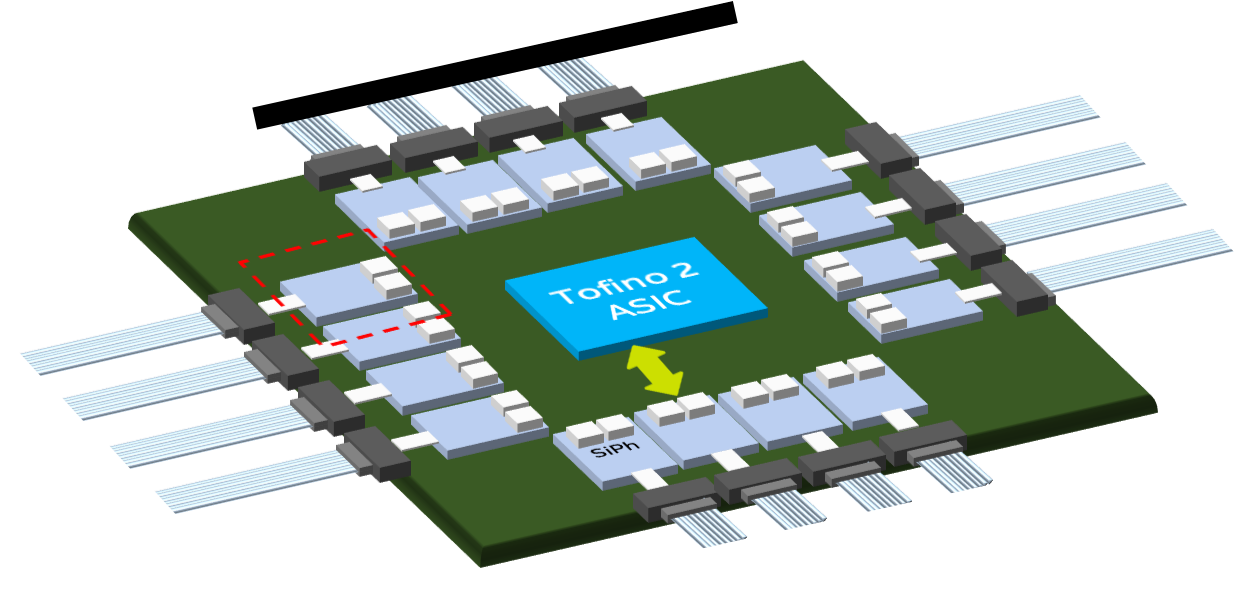
The design couples a Barefoot Tofino 2 switch chip to up to 16 optical ‘tiles’ - each tile, a 1.6-terabit silicon photonics die - for a total I/O of 25.6 terabits.
“It’s an easy upgrade to add our next-generation 25.6-terabit [switch chip] which is coming shortly,” says Ed Doe, Intel’s vice president, connectivity group, general manager, Barefoot division.
Intel acquired switch-chip maker, Barefoot, seven months ago after which it started the co-packaging optics project.
Intel also revealed that it is in the process of qualifying four new optical transceivers - a 400Gbase-DR4, a 200-gigabit FR4, a 100-gigabit FR1 and a 100Gbase-LR4 - to add to its portfolio of 100-gigabit PSM4 and CWDM4 modules.
Urgency
Intel had planned to showcase the working co-packaged switch at the OFC conference and exhibition, held last week in San Diego. But after withdrawing from the show due to the Coronavirus outbreak, Intel has continued to demonstrate the working co-packaged switch at its offices in Santa Clara.
 Hong Hou“We have some visionaries of the industry coming through and being very excited, making comments like: ‘This is an important milestone’,” says Hong Hou, corporate vice president, general manager, silicon photonics product division at Intel.
“There are a lot of doubts still [about co-packaged optics], in the reliability, the serviceability, time-to-market, and the right intercept point [when it will be needed]: is it 25-, 51- or 102-terabit switch chips?” says Hou. “But no one says this is not going to happen.”
If the timing for co-packaged optics remains uncertain, why the urgency?
“There has been a lot of doubters as to whether it is possible,” says Doe. “We had to show that this was feasible and more than just a demo.”
Intel has also been accumulating IP from its co-packaging work. Topics include the development of a silicon-photonics ring modulator, ensuring optical stability and signal integrity, 3D packaging, and passive optical alignment. Intel has also developed a fault-tolerant design that adds a spare laser to each tile to ensure continued working should the first laser fail.
“We can diagnose which laser is the source of the problem, and we have a redundant laser for each channel,” says Hou. “So instead of 16 lasers we have 32 functional lasers but, at any one time, only half are used.”
Co-packaged optics
Ethernet switches connected in the data centre currently use pluggable optics. The switch chip resides on a printed circuit board (PCB) and is interfaced to the pluggable modules via electrical traces.
But given that the capacity of the Ethernet switch ICs is doubling every two years, the power consumption of the I/O continues to rise yet the power delivered to a data centre is limited. Accordingly, solutions that ensure a doubling of switch speed but do not increase the power consumed are required.
One option is embedded optics such as the COBO initiative. Here, optics are moved from the switch’s faceplate onto the PCB, closer to the switch chip. This shortens the electrical traces while overcoming the capacity limitations of the number of pluggable modules that can be fitted onto the switch’s faceplate. Freeing up the faceplate by removing pluggables also improves airflow to cool the switch.
The second, more ambitious approach is co-packaged optics where optics are combined with the switch ASIC in the one package.
Co-packaged optics can increase the overall I/O on and off the switch chip, something that embedded optics doesn’t address. And placing the optics next to the ASIC, the drive requirements of the high-speed serialiser-deserialisers (serdes) is simplified.
Meanwhile, pluggable optics continue to advance in the form factors used and their speeds as well as developments such as fly-over cables that lower the loss connecting the switch IC to the front-panel pluggables.
In turn, certain hyperscalers are not convinced about co-packaged optics.
Microsoft and Facebook announced last year the formation of the Co-Packaged Optics (CPO) Collaboration to help guide the industry to develop the elements needed for packaging optics. But Google and Alibaba said at OFC that they prefer the flexibility and ease of maintenance of pluggables.
Data centre trends
The data centre is a key market for Intel which sells high-end server microprocessors, switch ICs, FPGAs and optical transceivers.
Large-scale data centres deploy 100,000 servers, 50,000 switches and over one million optical modules. And a million pluggable modules equate to $150M to $250M of potential revenue, says Intel.
 Ed Doe“One item that is understated is the [2:1] ratio of servers to switches,” says Doe. “We have seen a trend in recent years where the layers of switching in data centres have increased significantly.”
One reason for more switching layers is that traffic over-subscription is no longer used. With top-of-rack switches, a 3:1 over-subscription was common which limited the switch’s uplink bandwidth needed.
However, the changing nature of the computational workloads now requires that any server can talk to any other server.
“You can’t afford to have any over-subscription at any layer in the network,” says Doe. “As a result, you need to have a lot more bandwidth: an equal amount of downlink bandwidth to uplink bandwidth.”
Another factor that has increased the data centre’s switch layer count is the replacement of chassis switches with disaggregated pizza boxes. Typically, a chassis switch encompasses three layers of switching.
“Disaggregation is a factor but the big one is the 1:1 [uplink-downlink bandwidth] ratio, not just at the top-of-rack switch but all the way through,” says Doe. “They [the hyperscalers] want to have uniform bandwidth throughout the entire data centre.”
Tofino switch IC
Barefoot has two families of Tofino chips. The first-generation Tofino devices have a switching capacity ranging from 1.2 to 6.4 terabits and are implemented using a 16nm CMOS process. The Tofino 2 devices, implemented using a 7nm CMOS IC, range from 4 terabits to 12.8 terabits.
“What we having coming soon is the Tofino next-generation which will go to both 25 terabits and 51 terabits,” says Doe.
Intel is not discussing future products but Doe hints that both switch ICs will be announced jointly rather than the typical two-year delay between successive generations of switch IC. This also explains the urgency of the company’s co-packaging work.
The 12.8-terabit Tofino 2 chip comprises the switch core dies and four electrical I/O tiles that house the device’s serdes.
“The benefit of the tile design is that it allows us to easily swap the tiles for higher-speed serdes - 112 gigabit-per-second (Gbps) - once they become available,” says Doe. And switching the tiles to optical was already envisaged by Barefoot.
Optical tile
Intel’s 1.6-terabit silicon-photonics tile includes two integrated lasers (active and spare), a ring modulator, an integrated modulator driver, and receiver circuitry. “We also have on-chip a v-groove which allows for passive optical alignment,” says Hou.
Each tile implements the equivalent of four 400GBASE-DR4s. The 500m-reach DR4 comprises four 100-gigabit channels, each sent over single-mode fibre.
“This is a standards-based interface,” says Robert Blum, Intel’s director of strategic marketing and business development, as the switch chip must interact with standard-based optics.
The switch chip and the tiles sit on an interposer. Having an interposer will enable different tiles and different system-on-chips to be used in future.
Hou says that having the laser integrated with the tile saves power. This contrasts with designs where the laser is external to the co-packaged design.
The argument for using an external laser is that it is remote from the switch chip which runs hot. But Hou says that the switch chip itself has efficient thermal management which the tile and its laser(s) can exploit. Each tile consumes 35W, he says.
As for laser reliability, Intel points to its optical modules that it has been selling since 2016 when it started selling the PSM4.
Hou claims Intel’s hybrid laser design, where the gain chip is separated from the cavity, is far more reliable than a III-V facet cavity.
“We have shipped over three million 100-gigabit transceivers, primarily the PSM4. The DPM [defects per million] is 28-30, about two orders of magnitude less than our closest competitor,” says Hou. “Eight out of ten times the cause of the failure of a transceiver is the laser, and nine out of ten times, the laser failure is due to a cavity problem.”
The module’s higher reliability reduces the maintenance needed, and enables data centre operators to offer more stringent service-level agreements, says Hou.
Intel says it will adopt wavelength-division multiplexing (WDM) to enable a 3.2-terabit tile which will be needed with the 51.2-terabit Tofino.
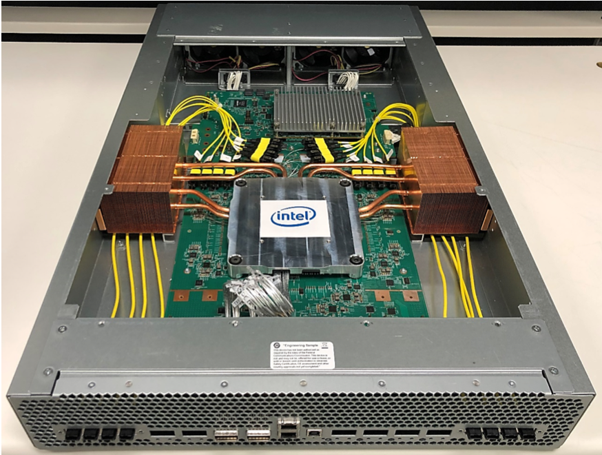 The Intel 12.8-terabit switch. The multi-chip package is below the heat sink that has the Intel logo. The two copper-coloured blocks are heat exchangers that provide cooling. The silver block at the back comprises a heat sink and an Intel processor that performs control-plane functions. And the front panel has both optical connectors (for the tiles) and pluggable cages. Source: Intel.
Switch platform
Intel’s 2-rack-unit (2RU) switch platform is a hybrid design: interfaced to the Tofino 2 are four tiles as well as fly-over cables to connect the chip to the front-panel pluggables.
“The hyperscalers are most interested in co-packaging but when you talk to enterprise equipment manufacturers, their customers may not have a fabric as complicated as that of the hyperscalers,” says Hou. “Bringing pluggables in there allows for a transition.”
The interposer design uses vertical plug-in connectors enabling a mix of optical and electrical interfaces “It is pretty easy, at the last minute, to [decide to] bring in 10 optical [interfaces] and six fly-over cables [to connect] to the pluggables,” says Hou.
“This is not like on-board optics,” adds Blum. “This [connector arrangement] is part of the multi-chip package, it doesn't go through the PCB. It allows us to have [OIF-specified] XSR serdes and get the power savings.”
Intel expects its co-packaged design to deliver a 30 per cent power saving as well as a 25 to 30 per cent cost-saving. And now that it has a working platform, Hou expects more engagements with customers that seeking these benefits and its higher-bandwidth density.
“This can stimulate more discussions and drive an ecosystem formation around this technology,” concludes Hou.
See Part 2: Ranovus outlines its co-packaged optics plans.