It's the second day of Christmastide and Sylvie Menezo is working: “I enjoyed the last two days and now I'm back at work.”
But then it should not be surprising given how Menezo is both the CEO and CTO of Scintil Photonics, the French start-up that secured €4.4 million in first-round funding last year.
 Sylvia Menezo, Scintil Photonics
Origins
Scintil Photonics’ expertise is in the design of silicon photonics circuits and the addition of active III-V materials - for lasing, gain and modulation - to a silicon substrate.
The start-up is using its funding to move its technology from the lab to production, working with an unnamed commercial foundry. The firm is also growing its staff, from eight to a dozen by the year-end.
Menezo worked previously at CEA-Leti, a French technology research institute, where her roles included heading the silicon photonics lab and business development.
In her business role, there was interest from customers in Leti’s silicon photonics technology but, at the time, its III-V technology on silicon was not ready.
“There was an opportunity of putting III-V on silicon but quite a bit of investment was needed to make the technology more mature,” she says. “This is where you need quick money and a 100 per cent dedicated team.”
Menezo discussed the idea of a start-up with CEA-Leti and once the organisation was satisfied that the proposed venture could succeed, it enabled her to step down to focus solely on developing the technology.
In return, the organisation that oversees Leti, CEA Tech, took a share in the start-up before it sought funding. This is one of CEA Tech’s duties, says Menezo, to create jobs.
“Once the patent technology was strengthened, we went outside and looked for funding,” she says.
Technology
Scintil Photonics has both indium phosphide and silicon photonics expertise. The start-up’s plans to develop and sell fully photonic integrated circuits (PICs). The start-up’s optical component library includes lasers, modulators, waveguides, wavelength filters, and photodetectors.
“We have a fabrication process which is CMOS-friendly and which relies on existing silicon-photonics technology,” says Menezo. “We want to have silicon and III-V fabricated and we want to commercialise photonic ICs.”
Scintil’s work with a commercial foundry will take its technology to production using a standard silicon photonics process.
 Source: Scintil Photonics
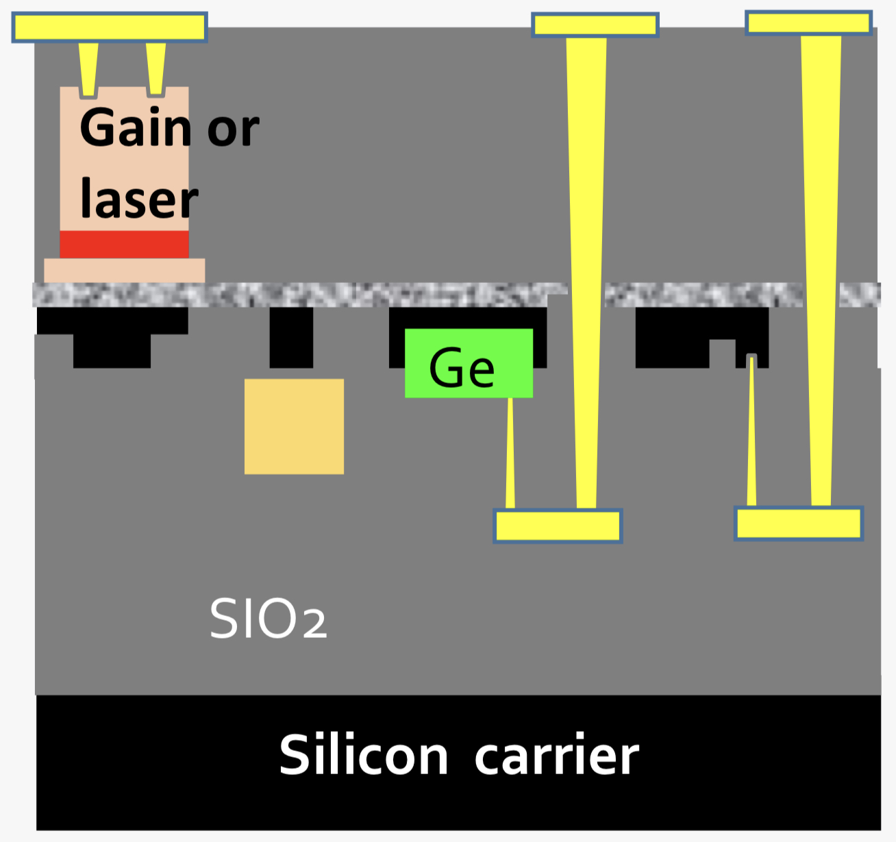
Once the silicon photonics chips are fabricated on a wafer, Scintil’s process bonds the wafer onto a silicon carrier, flips it and etches off the silicon-on-insulator (SOI) substrate.
Indium phosphide is bonded onto the exposed silicon layer before being processed to fabricate such active components as lasers, semiconductor optical amplifiers and hybrid modulators using CMOS fabrication techniques (see image).
Menezo describes the fabrication as CMOS-friendly: standard off-the-shelf processes are used while the processing of III-V is CMOS-compatible in terms of etching and electrical contacts.
Scintil’s process is also scalable, she says: new materials and functions will be added over time to the silicon photonics processes without impacting the integration of III-V materials onto the silicon.
“The more you design these devices and circuits, the more you see the design opportunities you have,” says Menezo. “This is the future if people manage to make it as a friendly as CMOS technology.”
Applications
Scintil Photonics is already working on circuit prototypes with the foundry.
The prototypes include coherent components for optical transmission and designs for 800-gigabit and 1.6-terabyte client-side interfaces. These are based on parallelising existing 400-gigabit DR4 and FR4 designs.
“For an 800-gigabit, the use of eight lanes [each lane being 100 gigabits] is indeed a good target because of [the need for] more integration,” says Menezo. “We can also scale to higher-speed lanes with our hybrid indium phosphide/ silicon photonics modulator.”
Eight-hundred gigabit modules are only needed from 2022 at the earliest.
Another application area for the technology is co-packaged optics, using optical interfaces to move data on- and off-chip.
Menezo says that the company is already thinking about the next round of funding but that it is at least two years away.