The second article in a series on co-packaged optics.
Part 2: Broadcom - a switch-chip vendor
The hyperscalers require ever more switching capacity in their data centres to scale the applications they run. A hierarchy of connected switches fitted with optical interfaces is used to provide the pathways that link the tens of thousands of servers found in data centres.
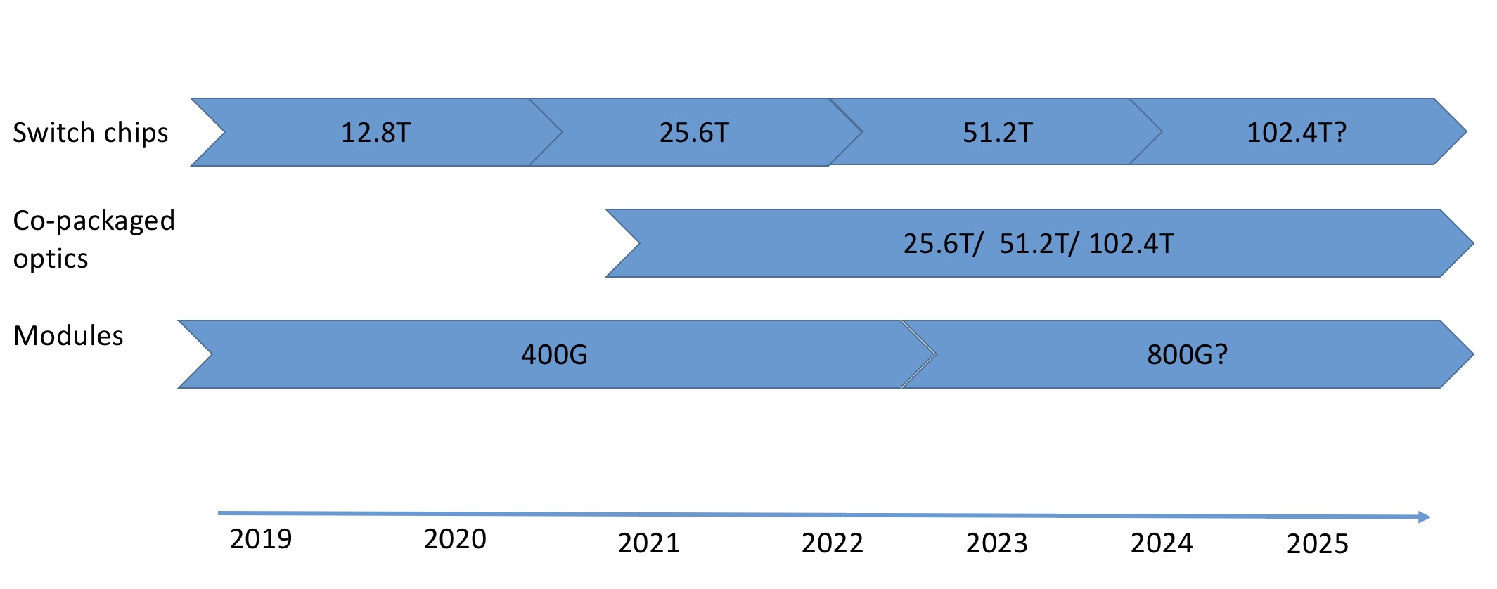
Silicon vendors are responding to this need by doubling the capacity of their switch chips every two years. The largest switch chips have a 12.8-terabit capacity and the first 25.6-terabit devices are expected next year. This relentless pace, however, is one that the optical module makers are struggling to match.
 Source: Gazettabyte
“It is a problem for the optics industry,” says Robert Stone, Distinguished Engineer at leading switch chip player, Broadcom. “The cadence at which we can evolve silicon generally moves a lot faster than the optics guys can monetise a generation of investment, and then reinvest it.”
Co-packaged optics
The result is a schism between the optics and the switch ICs, says Stone.
Data centre operators have had to use 100-gigabit interfaces across two generations of switching silicon. The lag between the two camps is also evident in how certain hyperscalers are adopting 200-gigabit pluggables as a stopgap measure before 400-gigabit modules become mainstream.
The doubling of chip capacity every two years will continue to challenge the optical module engineers. Can faster, power-hungry pluggable optical modules - 800-gigabit modules will follow 400-gigabit ones - fit on the faceplate of a switch at the density required? Currently, 32 400-gigabit optical modules fit on the front panel of a 1-rack-unit (1RU) switch. And if not, what are the alternatives to pluggable modules?
Two options are being pursued by the optical industry.
One is moving the optics from the switch’s front panel onto the motherboard. Such on-board optics shorten the length of the high-speed traces on the printed circuit board (PCB) linking the switch ASIC and the pluggable optics. In turn, the freed-up space on the front panel by ditching pluggables improves the ventilation and cooling of the switch.
The second option, co-packaged optics, places the optics with the ASIC in the same package.
Placing the optics next to the switch chip enables the high-speed serialiser-deserialiser (serdes), the circuit that gets data on and off the chip, to be simplified. No longer will the serdes have to drive very high-speed signals all the way to the front panel’s pluggables. This simplifies the PCB design, constrains the switch chip’s overall power consumption given how hundreds of serdes are used, and reduces the overall die area they consume.
It may just be that operators hedge their bets by deploying half co-packaged optics and half conventional optics to make sure they don’t completely strand themselves
At a recent panel session at the OFC show, held in San Diego in March, entitled Beyond 400G for Hyperscaler Data Centres, the consensus was that front-panel pluggable optics will continue for at least two more generations of switch chip: 25.6 terabits and 51.2 terabits.
“We can build such systems with conventional front-panel optics with a bit of hard work,” says Stone, a participant in the OFC panel discussion. For example, a 2RU-high 25.6-terabit switch platform will accommodate 64, 800-gigabit modules.
The ‘hard work’ refers to tackling the heat generated by the chip and, in particular, the power consumed all the serdes. But these are engineering challenges, not fundamental physics issues, they can be overcome, says Stone.
But there is an industry acceptance that continuing to increase the speed of client-side pluggables has a limited future and that change is coming.
Overlapping worlds
Stone’s belief is that co-packaged optics will first be deployed alongside pluggables, enabling the hyperscalars to deploy both technologies in their data centres. This will reduce the risk associated with introducing the new technology, such as a supply constraint or a reliability issue.
Indeed, this is the guidance Stone has been giving the silicon photonics players developing co-packaged optics. It is all well and good for a company to come up with very low power, dense wavelength grid optical interface design, he says, but the co-packaged device will need to interoperate with conventional front-panel pluggable optics.
“It may just be that operators hedge their bets by deploying half co-packaged optics and half conventional optics to make sure they don’t completely strand themselves,” says Stone.
Stone is confident that there will be co-packaged optics solutions with the advent of 25.6-terabit and 51.2-terabit switch chips.
“I don’t think they will be necessary,” he adds. “It will be more a cost and power optimisation in those generations.” But pursuing co-packaged optics provides a way for companies to differentiate themselves and innovate.
Stone also notes that certain switch chip vendors are separating the serdes input-output (I/O) circuitry, resulting in standalone dies that surround the packet-processing core. Such serdes ‘tiles’ lend themselves to a co-packaged design.
“Once you have split off the I/O, you may then switch the electrical I/O to optical I/O,” says Stone. “Obviously, there is a lot of detail to be worked out but the move away from a big monolithic-chip package makes it friendlier to do such integration.”
Unless there is a need to solve a feasibility challenge, designers will continue to cling to what they have done historically
Challenges
But co-packaged optics presents its own challenges.
Stone says that it is still uncertain whether co-packaged optics will be a must for the switch chip generation after 51.2 terabits although he believes that is when such optics becomes compelling.
“Having said that, it is not a complete slam-dunk in that generation either because now you are aggregating a lot of heat in a very small space,” he says. “If you take a 100-terabit chip, or whatever the number will be, and you pack all that optics onto it, trying to cool that is going to be very hard.” That suggests water-cooling will be needed as air-cooling will not be sufficient.
Unless there is a need to solve a feasibility challenge, designers will continue to cling to what they have done historically. “It is comfortable, people know how to do it, and the supply chain is already built up,” he says. All these factors change with the embrace of co-packaged optics.
The industry has yet to run into that feasibility gap but what has changed is that the industry now acknowledges that it is coming.
See also:
Part 1: Ayar Labs, click here