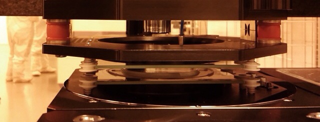
 X-Celeprint's micro transfer printing technology. Source: X-Celeprint
- X-Celeprint has a printing process that places individual 'chiplets' of III-V material onto silicon
- The micro transfer printing technique can be used to make silicon photonics circuits
- X-Celeprint will work with silicon photonics companies interested in licensing its technology
A key challenge facing silicon photonics players is creating a light source. Silicon does not lase so a III-V material is needed to form the laser.
One approach is to attach a tiny module holding the laser to the silicon photonics design. This is what the likes of Cisco Systems, Luxtera, Mellanox Technologies and IBM are doing: adding an external laser to the otherwise monolithic silicon photonics circuit.
An alternative technique is to bond the III-V material to the silicon and using photolithography and etching to construct the silicon photonics device. The attraction of III-V bonding is that the technique can be used to also make the modulators and photo-detectors. Known as heterogeneous integration, this approach is being used by companies such as Aurrion, Intel and Skorpios Technologies.
"Bonding is an elegant solution," says Roel Baets, a professor at the Photonics Research Group at Ghent University. "You can make the light source at the wafer scale and have a single chip solution that looks like a monolithic chip, including the light source."
Think of printing as pick-and-place in a massively parallel fashion. Instead of ink, we are picking up and printing arrays of high-performance semiconductors.
Bonding III-V material to silicon is itself non-trivial. First, silicon wafers are either 200mm or 300mm (8 or 12 inch) while III-V indium phosphide wafers are typically 50mm (2 inch). Indium phosphide wafers are also expensive, simply etching away the majority of the wafer to leave small islands of wanted material is hugely wasteful.
"There is only going to be a laser here or there, with a fill factor - an area coverage - of some one percent," says Baets. "You are throwing away a lot of III-V."
Equally, cutting up the III-V wafer into small slivers for bonding is complicated as it requires precision placement; a process difficult to automate to achieve high-yield circuits. This is the challenge the heterogeneous integration companies have set themselves.
It is a market opportunity identified by start-up X-Celeprint. It has a process that places individual 'chiplets' of III-V material onto silicon by the thousands.
X-Celeprint uses a micro transfer printing to place the chiplets onto silicon. "Think of printing as pick-and-place in a massively parallel fashion," says Kyle Benkendorfer, CEO of X-Celeprint. "Instead of ink, we are picking up and printing arrays of high-performance semiconductors."
Micro transfer printing is already used commercially to make high concentration solar cells, and it is being evaluated to place thin lasers on read/ write heads in disc drives. "We can print live devices or a slab of material on any substrate as long as it is flat," says Benkendorfer.
One benefit of the technique is that the thin III-V material is removed from the indium phosphide wafer but the underlying substrate is retained and can be recycled. For wafer-to-wafer bonding, in contrast, the substrate must be ground back. "This is several hundred microns of [substrate] material," says Benkendorfer. "With our process you can reprocess the wafer and regrow it, saving some $3,000."
The printing process also lends itself to automation. "We can very efficiently place active die of highly expensive compound material at the point of use, where it can then be converted into a device," he says.
X-Celeprint wants to work with silicon photonics companies interested in licensing its printing technology. Developing the process with a particular silicon photonics vendor takes time. Each application requires tailoring and it can take up to two years to make, test and scale up production, says the start-up.
"We recognise that silicon photonics as a large market is out there, no question," says Benkendorfer. "But the development time to get any significant market is going to be a while."