Feature
“This is a general rule: what starts as a series of parts loosely strung together, if used heavily enough, congeals into a self-contained unit.”
W. Brian Arthur, The Nature of Technology
 Infinera's Dave Welch: PICs are fibre-optic's current disruption
Dave Welch likes to draw a parallel with digital photography when discussing the use of photonic integration for optical networking. “The CMOS photodiode array – a photonic integrated circuit - changed the entire supply chain of photography,” says Welch, the chief strategy officer at Infinera.
Applied to networking, the photonic integrated circuit (PIC) is similar, argues Welch. It benefits system cost by integrating individual optical components but it delivers more. “All the value – inherently harder to pin down - of networking efficiency of a system that isn’t transponder-based,” says Welch.
Just how disruptive a technology the PIC proves to be is unclear but there is no doubting the growing role of optical integration.
“Integration is a key part of our thinking,” says Sam Bucci, vice president, WDM, Alcatel-Lucent’s optics activities. When designing a new platform, Alcatel-Lucent surveys components and techniques to identify disruptive technologies. Even if it chooses to implement functions using discrete components, the system is designed taking into account future integrated implementations.
“We are seeing interest [in photonic integration] across the spectrum," says Stefan Rochus, vice president of marketing and business development at CyOptics. "Long-haul, metro, access and chip-to-chip - everything is in play."
The drivers for optical integration’s greater use are harder to pin down.
Operators must contend with yearly data traffic growth estimated at between 45 to 65 percent yet their revenues are growing modestly. “It’s no secret that the capacity curve - whether the line side or the client side - is growing at an astonishing clip,” says Bucci.
The onus is thus on equipment and component makers to deliver platforms that reduce the transport cost per bit."Delivering more for less," says Graeme Maxwell, vice president of hybrid integration at CIP Technologies. “Space is a premium, power is an issue, operators want performance maintained or improved – all are driving integration.”
Cost is an issue for optical components with yearly price drops of 20 percent being common. “Hitting the cost-curve, we have run out of ways to do that with classic optics,” says Sinclair Vass, commercial director, EMEA at JDS Uniphase.
High-speed optical transmission at 40 and 100 Gigabit per second (Gbps) requires photonic integration though here the issues are as much performance as cost reduction. Indeed, its use can be viewed as the result of the integration between electronics and optics. To address optical signal impairments, chips must work at the edge of their performance, requiring the optical signal to be split into slower, parallel streams. Such an arrangement is ripe for photonic integration.
“It is as if there are two kinds of integration: at the boundary between optics and electronics, and the purely optical planar waveguide stuff,” says Karen Liu, vice president, components and video technologies at market research firm Ovum.
The other market where the full arsenal of optical integration techniques – hybrid and monolithic integration – is being applied is optical transceivers for passive optical networking (PON). Here the sole story is cost.
As old as the integrated circuit
Photonic integration is not new. The idea was first mooted in a 1969 AT&T Bell Labs’ paper that described how multiple miniature optical components could be interconnected via optical waveguides made using thin-film dielectric materials. But so far industry adoption for optical networking has been limited.

"Two kinds of integration: at the boundary between optics and electronics, and the purely optical planar waveguide stuff"
Karen Liu, Ovum
Heavy Reading, in a 2008 report, highlighted the limited progress made in photonic integration in recent years, with the exception of Infinera, a maker of systems based on a dense wavelength division multiplexing (DWDM) 10x10Gbps monolithically integrated PIC.
“Infinera has held very consistently to its original story, including sub-wavelength grooming, and have made progress over time,” says Liu. But she points out a real disruptive impact has not yet been seen: “The problem with the digital camera analogy is that something that is disruptive is not a straight replacement but implies the next step: changing the network architecture, not just how a system is implemented.”
On-off keying to phase modulation
One way operators are accommodating traffic growth is cramming more data down a fibre. It is this trend- from 10Gbps to 40 and 100Gbps lightpaths - that is spurring photonic integration.
“If you look at current 100 Gigabit, it is a bigger configuration than we would like,” says Joe Berthold, Ciena’s vice president of network architecture. Ciena’s first 100Gbps design requires three line cards, taking five inches of rack space, while its second-generation design will fit on a single, two-inch card.
Both 40 and 100Gbps transmissions must also operate over existing networks, matching the optical link performance of 10Gbps despite dispersion being more acute at higher line speeds. To meet the challenge, the industry has changed how it modulates data onto light. Whereas previous speed increments up to 10Gbps used simple on-off keying, 40 and 100Gbps use advanced modulation schemes based on phase, or phase combined with polarisation.
The modulation schemes split the optical signal into parallel paths to lower symbol rates. For example, 40Gbps differential quadrature phase-shift keying (DQPSK) uses two signals that effectively operating at 20 Gigabaud. Halving the rate relaxes the high-speed electronics requirements at the expense of complicating the optical circuitry.
The concept is extended further at 100Gbps. Here polarisation is combined with phase modulation (either DQPSK, or QPSK if coherent detection is used) such that four signals are used in parallel, each operating at 28 Gigabaud.

“The 40/100G area is shaping up to be the equivalent of breaking the sound barrier”
Brad Smith, LightCounting
“Optical integration is becoming a necessity because of 40 and 100 Gigabit [transmission],” says Berthold. “The modulation formats require you to deal with signals in parallel, and using non-integrated components explodes the complexity.”
The Optical Internetworking Forum organisation has chosen dual-polarisation QPSK (DP- QPSK) as the favoured modulation scheme for 100Gbps and has provided integrated transmitter and receiver module guidelines to encourage industry convergence on common components. In contrast, for 40Gbps several designs have evolved: differential phase-shift keying (DPSK) through to DQPSK and DP-QPSK.
Kim Roberts, Nortel's director of optics research, while acknowledging that optical integration benefits system footprint and cost, downplays its overall significance.
For him, the adoption of coherent systems for 40 and 100Gbps – Nortel was first to market with a 40Gbps DP-QPSK system – move the complexity ‘into CMOS’, leaving optics to perform the basic functions. “I don’t see an overwhelming argument for integration,” says Roberts. “It’s useful and shows up in lower cost and smaller designs but it’s not a revolution.”
Meanwhile, optical component companies are responding by integrating various building blocks to address the bulkier 40 and 100Gbps designs.
NeoPhotonics is now shipping two PICs for 40 and 100Gbps receivers: a DQPSK demodulator based on two delay-line interferometers (DLIs) and a coherent mixer for a DP-QPSK receiver.
The DLI, as implied by the name, delays one of the received symbols and compares it with the adjacent received one to uncover the phase-encoded information. This is then fed to a balanced detector - a photo-detector pair. For DQPSK, either two DLIs or a single DLI plus 90-degree hybrid are required along with two balanced receivers.
For 100Gbps, a DP-QPSK receiver has four channels - a polarisation beam splitter separates the two polarisations and each component is mixed with a component from a local reference signal using a 90-degree hybrid mixer. The two hybrid mixers decompose the referenced phase to intensity outputs representing the orthogonal phase components of the signal and the four differential outputs are fed into the four balanced detectors (Click here for OIF document and see Fig 5).
Neophotonics’ coherent mixer integrates monolithically all the demodulation functions between the polarisation beam splitter and the balanced photo-detectors.
The company has both indium phosphide and planar lightwave circuit (PLC) technology integration expertise but chose to implement its designs using PLC technology. “Indium phosphide is good for actives but is not good for passives and it is very expensive,” says Ferris Lipscomb, vice president of marketing at NeoPhotonics.
One benefit of using PLC for demodulation is that the signal path lengths need to have sub-millimeter accuracy to recover phase; implementing a discrete design using fibre to achieve such accuracy is clearly cumbersome.
Another development that reduces size and cost involves the teaming of u2t Photonics, a high-speed photo-detector and indium phosphide specialist, with Optoplex and Kylia, free-space optics DLI suppliers. The result is a compact DPSK receiver that combines the DLI and balanced receiver within one package. Such integration at the package level reduces the size since fibre routeing between separate DLI and detector packages is no longer needed. The receiver also cuts cost by a quarter, says u2t.
Jens Fiedler, vice president sales and marketing at u2t Photonics, acknowledges that the free-space DLI design may not be the most compact design but was chosen based on the status of the various technologies. “We needed to provide a solution and PLC was not ready,” he says.
u2t Photonics is investigating a waveguide-based DLI solution and is considering indium phosphide and, intriguingly, gallium arsenide. “Indium phosphide has the benefit of integrating the DLI with the balanced detector,” says Fiedler. “There are benefits but also technical challenges [with indium phosphide].”
At ECOC 2009 in September, u2t announced a multi-source agreement (MSA) with another detector specialist, Picometrix, which supports the OIF’s DP-QPSK coherent receiver design. The MSA defines the form factor, pin functions and locations, and functionality of the receiver package holding the balanced detectors, targeted at transponder and line card designs.
Photonic integration for high-speed transmissions is not confined to the receiver. Oclaro has developed a 40Gbps DQPSK monolithic modulator. Implemented in indium phosphide, the modulator could even be monolithically integrated with the laser but Oclaro has said that there are performance benefits such as signal strength in keeping the two separate.
Infinera, meanwhile, eschews transponders in favour of its 100Gbp indium phosphide-based PIC.
 Take your PIC
In September it announced a system for submarine transmission, achieved by adding a semiconductor optical amplifier (SOA) to its 10-channel transmitter and receiver PIC pair. “We are now at a point when the performance of the PIC is a good as the performance of discretes,” says Welch.
In March the company announced its next-gen PIC design - a 10x40Gbps DP-DQPSK transmitter and receiver chip pair. This is a significantly more complex design, with the transmitter integrating the equivalent of 300 optical functions; Infinera’s 10x10G transmitter PIC integrates 50.
Infinera favoured DP-DQPSK rather than the OIF-backed DP-QPSK as the latter requires significant chip support to perform the digital processing for signal recovery for each channel. Given the PIC’s 10 channels, the power consumption would be prohibitive. Instead Infinera tackles dispersion using a simpler, power-efficient optical design.
Is there a performance hit using DP-DQPSK? “There is a nominal industry figure, 1,600km reach being a good number,” says Welch. “For ultra long haul, we absolutely meet that.”
Infinera has still to launch the 400Gbps PIC whereas transponder-based system vendors have been shipping systems delivering 40Gbps lightpaths for several years. But the company says that the PIC exists, is working and all that is left is “managing it onto the manufacturing line”.
“The 40/100G area is shaping up to be the equivalent of breaking the sound barrier,” says Brad Smith, senior vice president at optical transceiver market research firm LightCounting. He questions the likely progress of optical component assemblies given they have far too many technical, cost, and size limitations. “PICs and silicon photonics have a shot at changing the game,” he says. “But the capital investment is very high with relatively low associated volumes.”
PON: an integration battleground
PON is one market where both hybrid and monolithic integration are competing with discrete-based optical transceiver designs. “Here the whole issue is cost – it’s not performance,” says Liu.
When Finisar entered the GPON transceiver market two years ago it conducted as survey as to what was available. What it found was revealing. “No-one was using the newer technologies, it was all the traditional technique based on TO cans,” said Julie Eng, vice president of optical engineering at Finisar. Mounted within the TO cans are active components such as a distributed-feedback (DFB) or Fabry-Perot laser, or a photo-detector. This is what integrated optics - whether a hybrid design basedon PLC or an indium phosphide monolithic PIC - is looking to displace.
“There is a huge infrastructure – millions of TO cans - and the challenge for hybrid and monolithic integration is that they are chasing a cost-curve that continues to come down,” says Eng.
According to NeoPhotonics’ Lipscomb, it is also hard for monolithic or hybrid integration to match the specifications of TO cans. “FTTx is similar to ROADMs, once one technology is established it is difficult for another to displace it,” he says.
But this is exactly what Canadian firms Enablence Technologies and OneChip Photonics are aiming to do.
Enablence, a hybrid integration specialist, uses a PLC-based design for PON. Onto the PLC are coupled a laser and detector for a diplexer PON design, or for a triplexer - two detectors. A common PLC optical platform is used for the different standards – Broadband PON, Ethernet PON (EPON) and Gigabit PON (GPON) - boosting unit volumes. All that is changed are the actives, for example a Fabry-Perot laser is added to the platform for 10km-reach EPON or a DFB for 20km GPON transceivers. Wavelength filtering is also performed using the PLC waveguides.
“Competing with TO cans in PON is challenging,” admits Matt Pearson, vice president of engineering at Enablence. That’s because the discrete design’s assembly is highly manual, benefiting from Far Eastern labour rates.
A hybrid approach brings several benefits, says Pearson: packaging a highly-integrated device is simpler compared to the numerous piece parts using TO cans. “It is also possible to seal at the chip level not at the module level, such that non-hermetic package can be used,” says Pearson.
There is also an additional, albeit indirect, benefit. Using hybrid integration, Enablence can reuse its intellectual property. “The same wafer process used for PON can be used for 40 and 100 Gig applications,” says Pearson. “These promise better margins as they are higher-end products.”
Enablence claims hybrid also scores when compared to monolithic integration. A hybrid design doesn’t sacrifice system performance: optimised lasers and detectors are used to meet the design specification. In contrast, performance compromises are inevitable for each of the optical functions – lasers, detectors, filtering - given that all are made in a single manufacturing process.
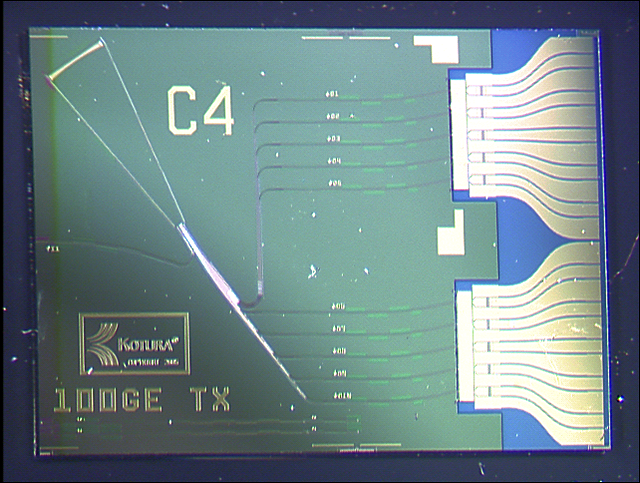
 OneChip's EPON diplexer PIC seated on a silicon optical bench and showing the connecting fibreOneChip counters by noting the cost benefits of monolithic integration: its EPON-based transceivers are claimed to be 25 percent cheaper than competing designs. “It is not just integration [and the compact design] but there is a completely different automated packaging of the transceiver,” says Andy Weirich, OneChip’s vice president of product line management.
The company also argues that all three approaches each have their particular compromises, and that all its optical functions are high performance: the company uses a DFB laser and an optically pre-amplified photo-detector for its designs. “If you can get the best specification with no additional cost, what advantage is there of buying a cheaper laser?” says Weirich.
“Inelegant as it is, the TO can’s performance is quite good as is its cost,” says Ovum’s Liu. What is evident here is how each company is coming from a different direction, she says: “Enablence points out that a discrete design is not a platform with a future whereas the likes of Finisar are saying: do we care?”
That said, Finisar’s Eng does expect photonic integration to be increasingly used for PON: “Its time will come, we are just not at that time now.”
Photonic integration will also be used in emerging standards such as wavelength division multiplexing PON (WDM-PON), especially at the head-end where the optical line terminal (OLT) resides.
“WDM-PON is very much point-to-point even though the fibre is shared like a normal PON,” says David Smith, CTO at CIP Technologies. “When you get in the central office there is a mass of equipment just like point-to-point [access].” The opportunity is to integrate the OLT’s lasers – typically 32 or 64 - into arrays, which will also save power, says Smith.
Tunables and interconnects
Other market segments are benefiting from photonic integration besides 40 and 100Gbps transmission and PON.
JDS Uniphase’s XFP module-based tunable laser is possible by monolithically integration the laser and Mach-Zehnder modulator. Not only is the resulting tunable laser compact – it is a few millimeters long - such that it and the associated electronics fit within the module, but the power consumption is below the pluggable’s 3.5W ceiling.
JDS Uniphase has also developed a compact optical amplifier that extends long-haul optical transmission before electrical signal regeneration is needed. A PLC chip is used to replace some 50 discrete optical components including isolators, photo-detectors for signal monitoring, a variable pump splitter and tunable gain-flattening and tilt filters.
The result is an amplifier halved in size and simpler to make since the PLC removes the need to route and splice fibres linking the discretes. Moreover, JDS Uniphase can use different PLC manufacturing masks to enable specific functions for particular customers. This is the closest the optical world gets to a programmable IC.
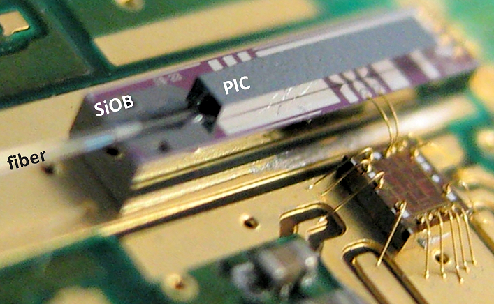
 Towards 1 terabit-per-second interfaces: a hybrid integrated prototype as part of an NIST project involving CyOptics and Kotura. Click on the photo for more details
The emerging 40 and 100 Gigabit Ethernet interface standards are another area suited for future integration. “What is driving optical integration here is size,” says Eng. “How do you fit 100Gigabit in a 3x5 inch module? That is cutting the size in half and will require a lot of R&D effort.”
In particular, optical integration will be needed to implement the 40GBASE-LR4 Gigabit Ethernet standard within a QSFP module. “You can’t fit four TO can lasers and four TO can receivers into a QSFP module,” says Rochus.
It is the 40 and 100 Gigabit Ethernet market that is the higher end market that also interests Enablence. “The drivers for PON and 100 Gigabit may be different but it’s the same PLC technology,” says Pearson. A PON diplexer may integrate one laser and one detector, for 100G it’s ten lasers and ten detectors, he says.
What next?
“Bandwidth growth is forcing us to consider architectures not considered before,” says Alcatel Lucent’s Bucci. The system vendor is accelerating its integration activities, whether it is integrating two wavelength-selective switches in a package or developing ‘electro-optic engines’ that combine advanced modulation optics and digital signal processing.
Moreover, operators themselves are more open to networking change due to the tremendous challenges they face, says Bucci: “They are being freed to do more, to take more risks.”
Welch believes one significant development that PICs will enable – perhaps a couple of years out - is adding and dropping at the packet level, at every site in the core network. “This will enable lots of reconfigurability and much finer granularity, delivering another level of networking efficiency,” he says.
Is this leading to disruption - the equivalent of digital cameras on handsets? Time will tell.
Click here for a mindmap of this article in PDF form.